R
XC18V00 Series In-System Programmable Configuration PROMs
Table 5 lists the IDCODE register values for the XC18V00
devices.
the XC18V00 device. If the device is blank or was not
loaded during programming, the USERCODE register con-
tains FFFFFFFFh.
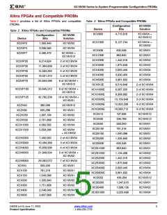
Table 5: IDCODES Assigned to XC18V00 Devices
XC18V00 TAP Characteristics
ISP-PROM
XC18V01
XC18V02
XC18V04
XC18V512
IDCODE
The XC18V00 family performs both in-system programming
and IEEE 1149.1 boundary-scan (JTAG) testing via a single
4-wire Test Access Port (TAP). This simplifies system
designs and allows standard Automatic Test Equipment to
perform both functions. The AC characteristics of the
XC18V00 TAP are described as follows.
05024093h or 05034093h
05025093h or 05035093h
05026093h or 05036093h
05023093h or 05033093h
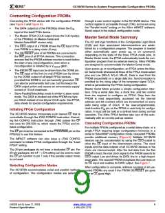
TAP Timing
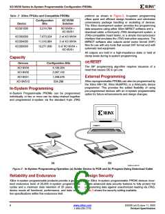
Figure 4 shows the timing relationships of the TAP signals.
These TAP timing characteristics are identical for both
boundary-scan and ISP operations.
The USERCODE instruction gives access to a 32-bit user
programmable scratch pad typically used to supply informa-
tion about the device’s programmed contents. By using the
USERCODE instruction, a user-programmable identifica-
tion code can be shifted out for examination. This code is
loaded into the USERCODE register during programming of
T
CKMIN1,2
TCK
TMS
T
T
MSS
MSH
T
T
DIH
DIS
TDI
T
DOV
TDO
DS026_04_032702
Figure 4: Test Access Port Timing
TAP AC Parameters
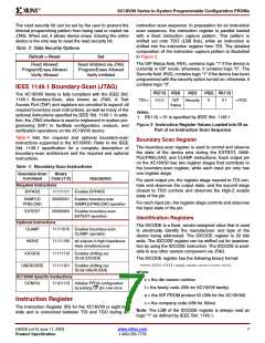
Table 6 shows the timing parameters for the TAP waveforms shown in Figure 4.
Table 6: Test Access Port Timing Parameters
Symbol
Parameter
TCK minimum clock period
Min
100
50
10
25
10
25
-
Max
Units
T
-
-
ns
ns
ns
ns
ns
ns
ns
CKMIN1
CKMIN2
T
TCK minimum clock period, Bypass Mode
TMS setup time
T
T
-
MSS
TMS hold time
-
MSH
T
TDI setup time
-
DIS
T
TDI hold time
-
DIH
T
TDO valid delay
25
DOV
8
www.xilinx.com
DS026 (v4.0) June 11, 2003
1-800-255-7778
Product Specification

 XILINX [ XILINX, INC ]