R
XC18V00 Series In-System Programmable Configuration PROMs
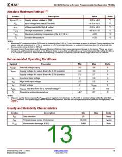
Absolute Maximum Ratings(1,2)
Symbol
Description
Supply voltage relative to GND
Value
–0.5 to +4.0
–0.5 to +5.5
–0.5 to +5.5
–65 to +150
+220
Units
V
V
V
CCINT/ CCO
V
Input voltage with respect to GND
Voltage applied to High-Z output
Storage temperature (ambient)
Maximum soldering temperature (10s @ 1/16 in.)
Junction temperature
V
IN
V
V
TS
T
T
°C
°C
°C
STG
SOL
T
+125
J
Notes:
1. Maximum DC undershoot below GND must be limited to either 0.5V or 10 mA, whichever is easier to achieve. During transitions, the
device pins can undershoot to –2.0V or overshoot to +7.0V, provided this over- or undershoot lasts less then 10 ns and with the
forcing current being limited to 200 mA.
2. Stresses beyond those listed under Absolute Maximum Ratings might cause permanent damage to the device. These are stress
ratings only, and functional operation of the device at these or any other conditions beyond those listed under Operating Conditions
is not implied. Exposure to Absolute Maximum Ratings conditions for extended periods of time might affect device reliability.
Recommended Operating Conditions
Symbol
Parameter
Min
3.0
3.0
2.3
0
Max
3.6
3.6
2.7
0.8
5.5
Units
V
V
Internal voltage supply
CCINT
V
Supply voltage for output drivers for 3.3V operation
Supply voltage for output drivers for 2.5V operation
Low-level input voltage
V
CCO
V
V
V
IL
V
High-level input voltage
2.0
0
V
IH
V
Output voltage
V
V
O
CCO
(1)
T
V
rise time from 0V to nominal voltage
CCINT
1
50
ms
C
VCC
T
Operating ambient temperature
–40°
85°
A
Notes:
1. At power up, the device requires the V
power supply to monotonically rise from 0V to nominal voltage within the specified
CCINT
V
rise time. If the power supply cannot meet this requirement, then the device might not perform power-on-reset properly. See
CCINT
Figure 8.
Quality and Reliability Characteristics
Symbol
Description
Min
20
Max
Units
Years
Cycles
Volts
T
Data retention
-
-
-
DR
N
Program/erase cycles (Endurance)
Electrostatic discharge (ESD)
20,000
2,000
PE
V
ESD
DS026 (v4.0) June 11, 2003
www.xilinx.com
13
Product Specification
1-800-255-7778

 XILINX [ XILINX, INC ]