R
XC18V00 Series In-System Programmable Configuration PROMs
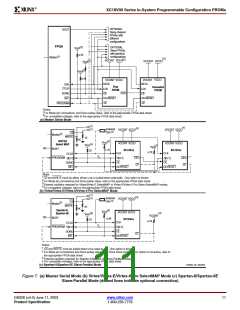
Reset Activation
On power up, OE/RESET is held low until the XC18V00 is
active (1 ms). OE/RESET is connected to an external resis-
tor to pull OE/RESET HIGH releasing the FPGA INIT and
allowing configuration to begin. If the power drops below
2.0V, the PROM resets. OE/RESET polarity is not program-
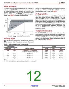
mable. See Figure 8 for power-up requirements.
remains in a high-impedance state regardless of the state of
the OE input. JTAG pins TMS, TDI and TDO can be in a
high-impedance state or High. See Table 7.
5V Tolerant I/Os
The I/Os on each re-programmable PROM are fully 5V tol-
erant even through the core power supply is 3.3V. This
allows 5V CMOS signals to connect directly to the PROM
inputs without damage. In addition, the 3.3V V
supply can be applied before or after 5V signals are applied
to the I/Os. In mixed 5V/3.3V/2.5V systems, the user pins,
power
3.6V
CCINT
Recommended Operating Range
3.0V
Recommended
the core power supply (V
), and the output power sup-
CCINT
ply (V
) can have power applied in any order. This
Rise
VCCINT
Time
CCO
makes the PROM devices immune to power supply
sequencing issues.
Customer Control Bits
0V
0ms 1ms
50ms
The XC18V00 PROMs have various control bits accessible
by the customer. These can be set after the array has been
programmed using “Skip User Array” in Xilinx iMPACT soft-
ware. The iMPACT software can set these bits to enable the
optional JTAG read security, parallel configuration mode, or
CF-->D4 pin function. See Table 7.
Time (ms)
ds026_10_061103
Figure 8: V
Power-Up Requirements
CCINT
Standby Mode
The PROM enters a low-power standby mode whenever
CE is asserted High. The address is reset. The output
Table 7: Truth Table for PROM Control Inputs
Control Inputs
Outputs
OE/RESET
CE
Internal Address
DATA
CEO
I
CC
(1)
High
Low
If address < TC : increment
Active
High-Z
High
Low
Active
Reduced
(1)
If address > TC : don’t change
Low
High
Low
Low
High
High
Held reset
Held reset
Held reset
High-Z
High-Z
High-Z
High
High
High
Active
Standby
Standby
Notes:
1. TC = Terminal Count = highest address value. TC + 1 = address 0.
12
www.xilinx.com
1-800-255-7778
DS026 (v4.0) June 11, 2003
Product Specification

 XILINX [ XILINX, INC ]