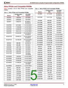
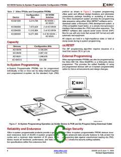
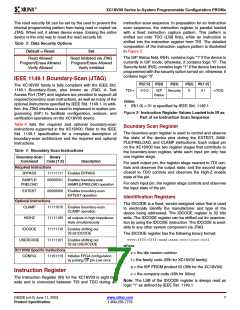
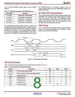
R
XC18V00 Series In-System Programmable Configuration PROMs
Table 1: Pin Names and Descriptions (Continued)
Boundary
20-pin
Pin
Name
Scan
Order
44-pin
VQFP
44-pin
PLCC
SOIC &
PLCC
Function
Pin Description
(1)
CF
22
21
DATA OUT Allows JTAG CONFIG instruction to
initiate FPGA configuration without
10
16
7
OUTPUT
powering down FPGA. This is an
ENABLE
open-drain output that is pulsed Low by
the JTAG CONFIG command.
CEO
12
11
DATA OUT Chip Enable Output (CEO) is connected
to the CE input of the next PROM in the
21
27
13
OUTPUT
chain. This output is Low when CE is Low
ENABLE
and OE/RESET input is High, AND the
internal address counter has been
incremented beyond its Terminal Count
(TC) value. CEO returns to High when
OE/RESET goes Low or CE goes High.
GND
TMS
GND is the ground connection.
6, 18, 28 &
41
3, 12, 24
& 34
11
5
MODE
SELECT
The state of TMS on the rising edge of
TCK determines the state transitions at
the Test Access Port (TAP) controller.
TMS has an internal 50K ohm resistive
pull-up on it to provide a logic “1” to the
device if the pin is not driven.
5
11
TCK
TDI
CLOCK
DATA IN
This pin is the JTAG test clock. It
sequences the TAP controller and all the
JTAG test and programming electronics.
7
3
13
9
6
4
This pin is the serial input to all JTAG
instruction and data registers. TDI has an
internal 50K ohm resistive pull-up on it to
provide a logic “1” to the system if the pin
is not driven.
TDO
DATA OUT This pin is the serial output for all JTAG
instruction and data registers. TDO has
an internal 50K ohm resistive pull-up on it
to provide a logic “1” to the system if the
pin is not driven.
31
37
17
(3)
V
Positive 3.3V supply voltage for internal
logic.
17, 35 &
38
23, 41 &
44
18 & 20
CCINT
(3)
(3)
V
Positive 3.3V or 2.5V supply voltage
connected to the input buffers and
8, 16, 26 & 14, 22, 32
19
CCO
(2)
36
& 42
output voltage drivers.
NC
No connects.
1, 2, 4,
1, 6, 7, 8,
11, 12, 20, 10,17, 18,
22, 23, 24, 26,28, 29,
30, 32, 33, 30,36, 38,
34, 37, 39, 39, 40, 43
44
Notes:
1. By default, pin 7 is the D4 pin in the 20-pin packages. However, CF --> D4 programming option can be set to override the default and route
the CF function to pin 7 in the Serial mode.
2. For devices with IDCODES 0502x093h, the input buffers are supplied by V
.
CCINT
3. For devices with IDCODES, 0503x093h, these V
pins are no connects: pin 38 in 44-pin VQFP package, pin 44 in 44-pin PLCC
CCINT
package and pin 20 in 20-pin SOIC and20-pin PLCC packages.
DS026 (v4.0) June 11, 2003
Product Specification
www.xilinx.com
1-800-255-7778
3

 XILINX [ XILINX, INC ]