R
XC18V00 Series In-System Programmable Configuration PROMs
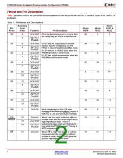
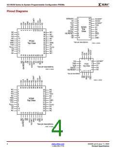
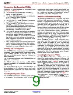
Pinout and Pin Description
Table 1 provides a list of the pin names and descriptions for the 44-pin VQFP and PLCC and the 20-pin SOIC and PLCC
packages.
Table 1: Pin Names and Descriptions
Boundary
Scan
Order
20-pin
SOIC &
PLCC
Pin
Name
44-pin
VQFP
44-pin
PLCC
Function
Pin Description
D0
D1
D2
D3
D4
D5
D6
D7
CLK
4
3
DATA OUT D0 is the DATA output pin to provide data
40
29
42
27
9
2
1
for configuring an FPGA in serial mode.
OUTPUT
ENABLE
6
5
DATA OUT D0-D7 are the output pins to provide
parallel data for configuring a Xilinx
35
4
16
2
OUTPUT
ENABLE
FPGA in Slave-Parallel/SelectMap mode.
D1-D7 remain in HIGHZ state when the
PROM operates in serial mode.
2
1
DATA OUT
D1-D7 can be left unconnected when the
PROM is used in serial mode.
OUTPUT
ENABLE
8
7
DATA OUT
33
15
31
20
25
15
OUTPUT
ENABLE
(1)
24
23
DATA OUT
7
OUTPUT
ENABLE
10
9
DATA OUT
25
14
19
14
9
OUTPUT
ENABLE
17
16
DATA OUT
OUTPUT
ENABLE
14
13
DATA OUT
12
OUTPUT
ENABLE
0
DATA IN
Each rising edge on the CLK input
increments the internal address counter if
both CE is Low and OE/RESET is High.
43
13
5
3
8
OE/
RESET
20
19
18
DATA IN
When Low, this input holds the address
counter reset and the DATA output is in a
high-impedance state. This is a
19
DATA OUT
bidirectional open-drain pin that is held
Low while the PROM is reset. Polarity is
NOT programmable.
OUTPUT
ENABLE
CE
15
DATA IN
When CE is High, the device is put into
low-power standby mode, the address
counter is reset, and the DATA pins are
put in a high-impedance state.
15
21
10
2
www.xilinx.com
DS026 (v4.0) June 11, 2003
1-800-255-7778
Product Specification

 XILINX [ XILINX, INC ]