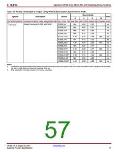
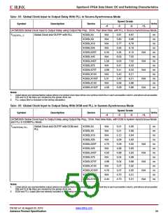
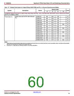
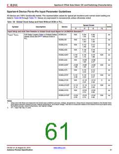
Spartan-6 FPGA Data Sheet: DC and Switching Characteristics
Spartan-6 Device Pin-to-Pin Input Parameter Guidelines
All devices are 100% functionally tested. The representative values for typical pin locations and normal clock loading are
listed in Table 68 through Table 74. Values are expressed in nanoseconds unless otherwise noted.
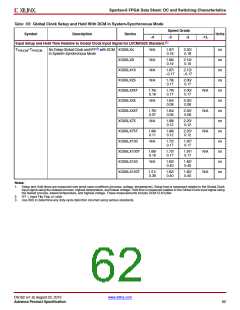
Table 68: Global Clock Setup and Hold Without DCM or PLL
Speed Grade
Symbol
Description
Device
Units
-4
Input Setup and Hold Time Relative to Global Clock Input Signal for LVCMOS25 Standard.(1)
-3
-2
-1L
TPSFD/ TPHFD
Full Delay (Legacy Delay or Default Delay) XC6SLX4
Global Clock and IFF(2) without DCM or
N/A
N/A
N/A
N/A
0.34/
1.54
0.34/
1.59
ns
ns
ns
ns
ns
ns
ns
ns
ns
ns
ns
ns
ns
PLL
XC6SLX9
0.31/
1.40
0.31/
1.49
XC6SLX16
XC6SLX25
XC6SLX25T
XC6SLX45
XC6SLX45T
XC6SLX75
XC6SLX75T
XC6SLX100
XC6SLX100T
XC6SLX150
XC6SLX150T
0.12/
1.48
0.12/
1.64
0.18/
1.75
0.18/
1.99
0.18/
1.64
0.18/
1.75
0.18/
1.99
N/A
N/A
N/A
–0.08/
1.95
–0.08/
2.27
–0.08/
1.88
–0.08/
1.95
–0.08/
2.27
N/A
0.13/
2.29
0.13/
2.57
0.13/
2.08
0.13/
2.29
0.13/
2.57
N/A
0
N/A
–0.14/
2.24
–0.14/
2.56
–0.14/
2.15
–0.14/
2.24
–0.14/
2.56
N/A
N/A
–0.24/
2.74
–0.24/
2.95
–0.24/
2.55
–0.24/
2.74
–0.24/
2.95
N/A
Notes:
1. Setup and Hold times are measured over worst case conditions (process, voltage, temperature). Setup time is measured relative to the Global Clock
input signal using the slowest process, highest temperature, and lowest voltage. Hold time is measured relative to the Global Clock input signal using
the fastest process, lowest temperature, and highest voltage.
2. IFF = Input Flip-Flop or Latch.
DS162 (v1.9) August 23, 2010
www.xilinx.com
Advance Product Specification
61

 XILINX [ XILINX, INC ]