R
Platform Flash In-System Programmable Configuration PROMs
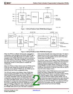
X-Ref Target - Figure 1
CLK CE
OE/RESET
TCK
TMS
TDI
Data
Control
and
JTAG
CEO
Serial
Memory
Interface
Data
DATA (D0)
Serial Mode
Address
Interface
TDO
CF
ds123_01_30603
Figure 1: XCFxxS Platform Flash PROM Block Diagram
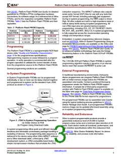
X-Ref Target - Figure 2FI
CLK
CE
EN_EXT_SEL
OE/RESET BUSY
OSC
CLKOUT
CEO
Decompressor
Control
and
JTAG
Serial
or
Parallel
Interface
TCK
TMS
TDI
Data
Memory
DATA (D0)
(Serial/Parallel Mode)
Address
TDO
Interface
Data
D[1:7]
(Parallel Mode)
DS123_19_031908
CF
REV_SEL [1:0]
Figure 2: XCFxxP Platform Flash PROM Block Diagram
When the FPGA is in Master Serial mode, it generates a
configuration clock that drives the PROM. With CF High, a
short access time after CE and OE are enabled, data is
available on the PROM DATA (D0) pin that is connected to
the FPGA DIN pin. New data is available a short access
time after each rising clock edge. The FPGA generates the
appropriate number of clock pulses to complete the
configuration.
short access time after each rising clock edge. The data is
clocked into the FPGA on the following rising edge of the
CCLK. A free-running oscillator can be used in the Slave
Parallel/Slave SelectMAP mode.
The XCFxxP version of the Platform Flash PROM provides
additional advanced features. A built-in data decompressor
supports utilizing compressed PROM files, and design
revisioning allows multiple design revisions to be stored on
a single PROM or stored across several PROMs. For design
revisioning, external pins or internal control bits are used to
select the active design revision.
When the FPGA is in Slave Serial mode, the PROM and the
FPGA are both clocked by an external clock source, or
optionally, for the XCFxxP PROM only, the PROM can be
used to drive the FPGA’s configuration clock.
Multiple Platform Flash PROM devices can be cascaded to
support the larger configuration files required when
targeting larger FPGA devices or targeting multiple FPGAs
daisy chained together. When utilizing the advanced
features for the XCFxxP Platform Flash PROM, such as
design revisioning, programming files which span cascaded
PROM devices can only be created for cascaded chains
containing only XCFxxP PROMs. If the advanced XCFxxP
features are not enabled, then the cascaded chain can
include both XCFxxP and XCFxxS PROMs.
The XCFxxP version of the Platform Flash PROM also
supports Master SelectMAP and Slave SelectMAP (or
Slave Parallel) FPGA configuration modes. When the FPGA
is in Master SelectMAP mode, the FPGA generates a
configuration clock that drives the PROM. When the FPGA
is in Slave SelectMAP Mode, either an external oscillator
generates the configuration clock that drives the PROM and
the FPGA, or optionally, the XCFxxP PROM can be used to
drive the FPGA’s configuration clock. With BUSY Low and
CF High, after CE and OE are enabled, data is available on
the PROMs DATA (D0-D7) pins. New data is available a
DS123 (v2.18) May 19, 2010
www.xilinx.com
Product Specification
2

 XILINX [ XILINX, INC ]