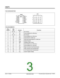
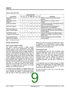
X9279
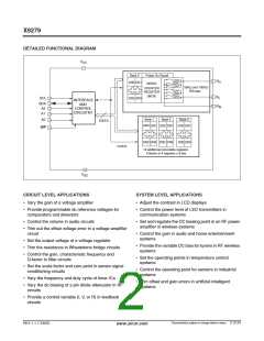
DETAILED FUNCTIONAL DIAGRAM
V
CC
Bank 0
Power On Recall
WIPER
R
H
DR0 DR1
50KΩ and 100KΩ
COUNTER
REGISTER
(WCR)
256-taps
R
R
L
SCL
DR2 DR3
INTERFACE
AND
CONTROL
SDA
A2
W
CIRCUITRY
A1
Bank 1
DR0
A0
Bank 2
Bank 3
DATA
DR1 DR0 DR1
DR0 DR1
WP
DR2 DR3 DR2 DR3
DR2 DR3
Control
12 additional nonvolatile registers
3 Banks of 4 registers x 8-bits
V
SS
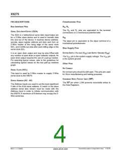
CIRCUIT LEVEL APPLICATIONS
SYSTEM LEVEL APPLICATIONS
• Vary the gain of a voltage amplifier
• Adjust the contrast in LCD displays
• Provide programmable dc reference voltages for
comparators and detectors
• Control the power level of LED transmitters in
communication systems
• Control the volume in audio circuits
• Set and regulate the DC biasing point in an RF power
amplifier in wireless systems
• Trim out the offset voltage error in a voltage amplifier
circuit
• Control the gain in audio and home entertainment
systems
• Set the output voltage of a voltage regulator
• Provide the variable DC bias for tuners in RF wireless
systems
• Trim the resistance in Wheatstone bridge circuits
• Control the gain, characteristic frequency and
Q-factor in filter circuits
• Set the operating points in temperature control
systems
• Set the scale factor and zero point in sensor signal
conditioning circuits
• Control the operating point for sensors in industrial
systems
• Vary the frequency and duty cycle of timer ICs
• Trim offset and gain errors in artificial intelligent
systems
• Vary the dc biasing of a pin diode attenuator in RF
circuits
• Provide a control variable (I, V, or R) in feedback
circuits
Characteristics subject to change without notice. 2 of 24
REV 1.1.7 2/6/03
www.xicor.com

 XICOR [ XICOR INC. ]