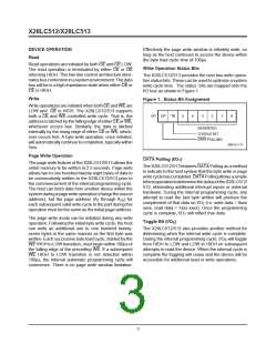
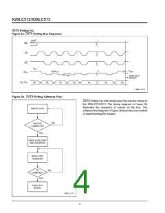
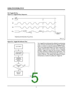
X28LC512/X28LC513
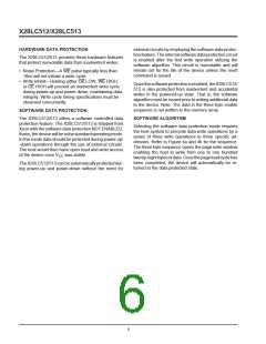
Software Data Protection
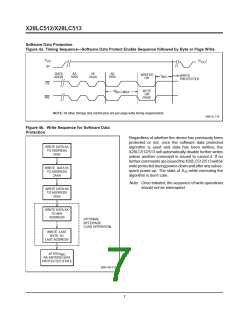
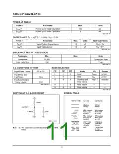
Figure 4a. Timing Sequence—Software Data Protect Enable Sequence followed by Byte or Page Write
V
(V
)
CC
0V
CC
DATA
ADDR
AA
5555
55
2AAA
A0
5555
WRITES
OK
t
WRITE
PROTECTED
WC
CE
≤t
BYTE
OR
PAGE
BLC MAX
WE
NOTE: All other timings and control pins are per page write timing requirements.
3005 ILL F16
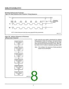
Figure 4b. Write Sequence for Software Data
Protection
Regardless of whether the device has previously been
protected or not, once the software data protected
algorithm is used and data has been written, the
X28LC512/513 will automatically disable further writes
unless another command is issued to cancel it. If no
further commands are issued the X28LC512/513 will be
writeprotectedduringpower-downandafteranysubse-
WRITE DATA AA
TO ADDRESS
5555
WRITE DATA 55
TO ADDRESS
2AAA
quent power-up. The state of A while executing the
15
algorithm is don’t care.
Note: Once initiated, the sequence of write operations
should not be interrupted.
WRITE DATA A0
TO ADDRESS
5555
WRITE DATA XX
TO ANY
ADDRESS
OPTIONAL
BYTE/PAGE
LOAD OPERATION
WRITE LAST
BYTE TO
LAST ADDRESS
AFTER t
RE-ENTERS DATA
WC
PROTECTED STATE
3005 FHD F17
7

 XICOR [ XICOR INC. ]