X28LC512/X28LC513
The Toggle Bit I/O
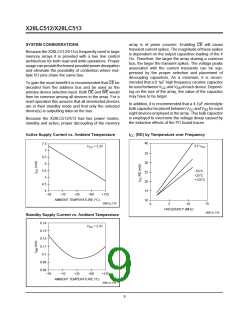
6
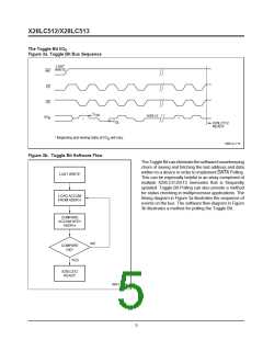
Figure 3a. Toggle Bit Bus Sequence
LAST
WRITE
WE
CE
OE
V
OH
HIGH Z
I/O
6
*
*
V
OL
X28LC512
READY
* Beginning and ending state of I/O will vary.
6
3005 ILL F14
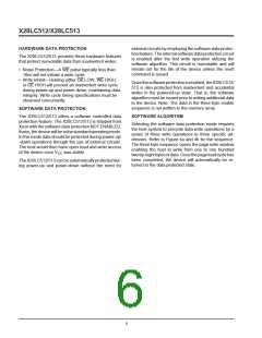
Figure 3b. Toggle Bit Software Flow
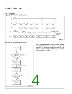
TheToggleBitcaneliminatethesoftwarehousekeeping
chore of saving and fetching the last address and data
written to a device in order to implement DATA Polling.
This can be especially helpful in an array comprised of
multiple X28LC512/513 memories that is frequently
updated. Toggle Bit Polling can also provide a method
for status checking in multiprocessor applications. The
timing diagram in Figure 3a illustrates the sequence of
events on the bus. The software flow diagram in Figure
3b illustrates a method for polling the Toggle Bit.
LAST WRITE
LOAD ACCUM
FROM ADDR n
COMPARE
ACCUM WITH
ADDR n
NO
COMPARE
OK?
YES
X28LC512
READY
3005 ILL F15
5

 XICOR [ XICOR INC. ]