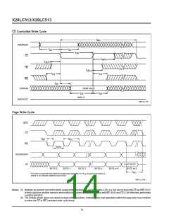
X28LC512/X28LC513
ABSOLUTE MAXIMUM RATINGS*
*COMMENT
Temperature under Bias
Stresses above those listed under “Absolute Maximum
Ratings” may cause permanent damage to the device.
This is a stress rating only and the functional operation of
the device at these or any other conditions above those
indicatedintheoperationalsectionsofthisspecificationis
not implied. Exposure to absolute maximum rating condi-
tions for extended periods may affect device reliability.
X28LC512/513............................. –10°C to +85°C
X28LC512I/X28LC513I.............. –65°C to +135°C
Storage Temperature ....................... –65°C to +150°C
Voltage on any Pin with
Respect to V
....................................... –1V to +7V
SS
D.C. Output Current ............................................. 5mA
Lead Temperature
(Soldering, 10 seconds).............................. 300°C
RECOMMEND OPERATING CONDITIONS
Supply Voltage
Limits
Temperature
Min.
Max.
X28LC512/513
3.3V ±10%
Commercial
Industrial
0°C
+70°C
+85°C
3005 PGM T03.1
–40°C
3005 PGM T02
D.C. OPERATING CHARACTERISTICS (Over recommended operating conditions, unless otherwise specified.)
Limits
Symbol
Parameter
Min.
Max.
Units
Test Conditions
I
V
Current (Active)
25
mA CE = OE = V , WE = V ,
CC
SB
CC
IL
IH
(CMOS Inputs)
All I/O’s = Open, Address Inputs =
0.1xV /0.9xV Levels
CC
CC
@ f = 5MHz
I
V
CC
Current (Standby)
150
µA
OE = V , CE = V – 0.3V
IL CC
(CMOS Inputs)
All I/O’s = Open, Other Inputs = V
IH
I
I
Input Leakage Current
Output Leakage Current
Input LOW Voltage
Input HIGH Voltage
Output LOW Voltage
Output HIGH Voltage
10
10
µA
µA
V
V
V
= V to V
SS CC
LI
IN
= V to V , CE = V
CC
LO
OUT
SS
CC
(1)
V
V
V
V
–1
2
0.6
lL
(1)
VCC + 0.5
0.4
V
IH
V
I = 1mA
OL
OL
OH
2.4
V
I = –200µA
OH
3005 PGM T04.2
Notes: (1) V min. and V max. are for reference only and are not tested.
IL
IH
10

 XICOR [ XICOR INC. ]