X28LC512/X28LC513
POWER-UP TIMING
Symbol
Parameter
Max.
Units
(2)
t
t
Power-up to Read Operation
Power-up to Write Operation
100
5
µs
PUR
(2)
ms
PUW
3005 PGM T05
CAPACITANCE T = +25°C, f = 1MHz, V = 3.3V
A
CC
Symbol
Parameter
Max.
Units
Test Conditions
(2)
C
C
Input/Output Capacitance
Input Capacitance
10
10
pF
pF
V
V
= 0V
= 0V
I/O
I/O
(2)
IN
IN
3005 PGM T06.1
ENDURANCE AND DATA RETENTION
Parameter
Min.
Max.
Units
Endurance
10,000
100
Cycles per Byte
Years
Data Retention
3005 PGM T11
A.C. CONDITIONS OF TEST
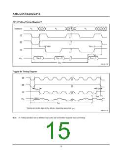
MODE SELECTION
Input Pulse Levels
0V to 3V
CE
L
OE
L
WE
H
Mode
Read
Write
I/O
Power
Active
D
OUT
IN
Input Rise and
Fall Times
L
H
L
D
Active
10ns
1.5V
H
X
X
Standby and
Write Inhibit
High Z
Standby
Input and Output
Timing Levels
3856 PGM T07.1
X
X
L
X
H
Write Inhibit
Write Inhibit
—
—
—
X
—
3005 PGM T08
EQUIVALENT A.C. LOAD CIRCUIT
SYMBOL TABLE
5V
WAVEFORM
INPUTS
OUTPUTS
2.66KΩ
Must be
steady
Will be
steady
OUTPUT
May change
from LOW
to HIGH
Will change
from LOW
to HIGH
4.46KΩ
30pF
May change
from HIGH
to LOW
Will change
from HIGH
to LOW
3005 ILL F21.3
Don’t Care:
Changes
Allowed
Changing:
State Not
Known
N/A
Center Line
is High
Impedance
Note: (2) This parameter is periodically sampled and not 100%
tested.
11

 XICOR [ XICOR INC. ]