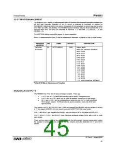
Product Preview
WM8983
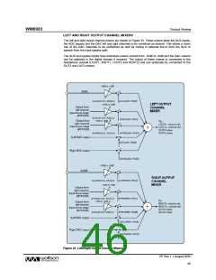
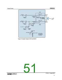
HEADPHONE OUTPUTS (LOUT1 AND ROUT1)
The headphone outputs LOUT1 and ROUT1 can drive a 16Ω or 32Ω headphone load, either through
DC blocking capacitors, or DC-coupled to a buffered midrail reference as shown in Figure 24. OUT3,
OUT4, LOUT2 or ROUT2 could be used as this buffered reference if one of these outputs is not
being used, saving decoupling capacitors, at the expense of increased power consumption. For fully
independent left and right channels, two separate midrail references can be used, eliminating
crosstalk caused by headphone ground impedances, at the expense of increased power
consumption.
Headphone Output using DC Blocking Capacitors:
Lowest power consumption (Two outputs enabled);
Large and expensive capacitors;
Bass response may be reduced for smaller capacitors;
Impedance in common ground may introduce crosstalk.
DC Coupled Headphone Output:
Higher power consumption (Three outputs enabled);
Improved PSRR if AVDD2 connected to AVDD1;
Impedance in common ground may introduce crosstalk;
Improved bass response (DC connection).
DC Coupled with Fully Independent Left / Right Drive:
Highest power consumption (Four outputs enabled);
Improved PSRR if AVDD2 connected to AVDD1;
Independent L/R pseudo-ground eliminates crosstalk;
Improved bass response (DC connection);
Non-standard headphone connection may not be suitable
for some applications.
Figure 24 Recommended Headphone Output Configurations
Each headphone output has an analogue volume control PGA with a gain range of -57dB to +6dB.
When DC blocking capacitors are used, their capacitance and the load resistance together
determine the lower cut-off frequency of the output signal, fc. Increasing the capacitance lowers fc,
improving the bass response. Smaller capacitance values will diminish the bass response.
Assuming a 16Ω load and C1, C2 = 220µF:
fc = 1 / 2π RLC1 = 1 / (2π x 16Ω x 220µF) = 45 Hz
In the DC coupled configuration, the headphone “ground” is connected to the VMID pin. The
OUT3/4 pins can be configured as a DC output driver by setting the OUT3MUTE and OUT4MUTE
register bit. The DC voltage on VMID in this configuration is equal to the DC offset on the LOUT1
and ROUT1 pins therefore no DC blocking capacitors are required. This saves space and material
cost in portable applications.
Note that LOUT2, ROUT2, OUT3 and OUT4 have an optional output boost of 1.5x. When these are
configured in this output boost mode (SPKBOOST/OUT3BOOST/OUT4BOOST=1) then the VMID
value of these outputs will be equal to 1.5xAVDD/2 and will not match the VMID of the headphone
drivers. Do not use the DC coupled output mode in this configuration.
It is recommended to connect the DC coupled outputs only to headphones, and not to the line input
of another device. Although the built-in short circuit protection will prevent any damage to the
headphone outputs, such a connection may be noisy, and may not function properly if the other
device is grounded.
PP Rev 1.1 August 2005
49
w

 WOLFSON [ WOLFSON MICROELECTRONICS PLC ]