Pre-Production
WM8959
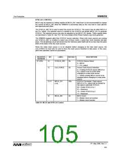
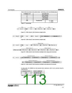
CLASS D SWITCHING CLOCK
The Class D switching clock is derived from SYSCLK as determined by register field DCLKDIV as
described in Table 61. This clock should be set to between 700kHz and 800kHz for optimum
performance. The class D switching clock should not be disabled when the speaker output is active,
as this will prevent the speaker outputs from functioning. The class D switching clock frequency
should not be altered while the speaker output is active as this may generate an audible click.
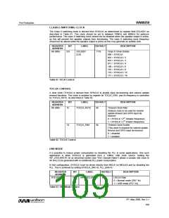
REGISTER
ADDRESS
BIT
8:6
LABEL
DEFAULT
DESCRIPTION
R6 (06h)
DCLKDIV
[2:0]
111b
Class D Clock Divider
000 = SYSCLK
001 = SYSCLK / 2
010 = SYSCLK / 3
011 = SYSCLK / 4
100 = SYSCLK / 6
101 = SYSCLK / 8
110 = SYSCLK / 12
111 = SYSCLK / 16
Table 61 DCLK Control
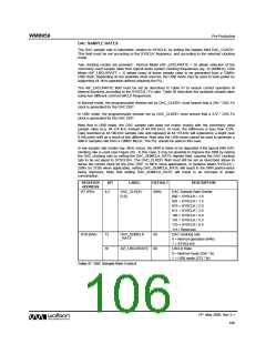
TOCLK CONTROL
A slow clock (TOCLK) is derived from SYSCLK to enable input de-bouncing and volume update
timeout functions. This clock is enabled by register bit TOCLK_ENA, and its frequency is controlled
by TOCLK_RATE, as described in Table 62.
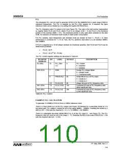
REGISTER
ADDRESS
BIT
15
LABEL
DEFAULT
DESCRIPTION
R6 (06h)
TOCLK_RATE
0b
Timeout Clock Rate
(Selects clock to be used for volume
update timeout and GPIO input de-
bounce)
0 = SYSCLK / 221 (Slower Response)
1 = SYSCLK / 219 (Faster Response)
Timeout Clock Enable
14
TOCLK_ENA
0b
(This clock is required for volume update
timeout and GPIO input de-bounce)
0 = disabled
1 = enabled
Table 62 TOCLK Control
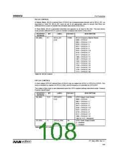
USB MODE
It is possible to reduce power consumption by disabling the PLL in some applications. One such
application is when SYSCLK is generated from a 12MHz USB clock source. Setting the
AIF_LRCLKRATE bit as described earlier (see “DAC Sample Rates”) allows a sample rate close to
44.1kHz to be generated with no additional PLL power consumption.
In this configuration, SYSCLK must be driven directly from MCLK (or MCLK2) and by disabling the
PLL. This is achieved by setting SYSCLK_SRC=0, PLL_ENA=0.
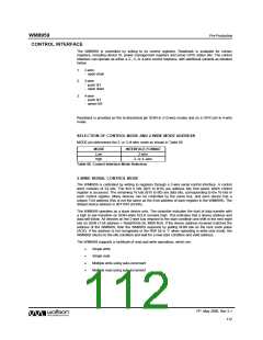
REGISTER
ADDRESS
BIT
LABEL
DEFAULT
DESCRIPTION
R10 (0Ah)
10
AIF_LRCLKRATE
0b
LRCLK Rate
0 = Normal mode (256 * fs)
1 = USB mode (272 * fs)
Table 63 USB Mode Control
PP, May 2008, Rev 3.1
109
w

 WOLFSON [ WOLFSON MICROELECTRONICS PLC ]