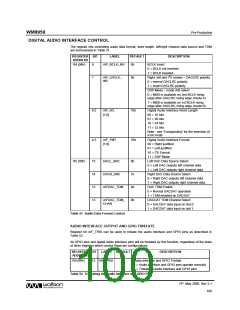
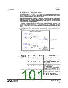
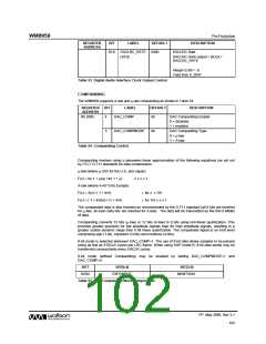
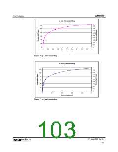
WM8959
Pre-Production
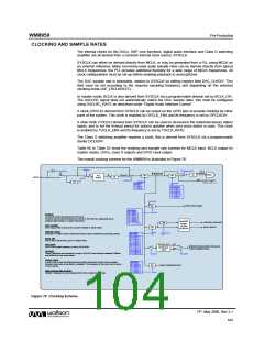
CLOCKING AND SAMPLE RATES
The internal clocks for the DACs, DSP core functions, digital audio interface and Class D switching
amplifier are all derived from a common internal clock source, SYSCLK.
SYSCLK can either be derived directly from MCLK, or may be generated from a PLL using MCLK as
an external reference. Many commonly-used audio sample rates can be derived directly from typical
MCLK frequencies; the PLL provides additional flexibility for a wide range of MCLK frequencies. All
clock configurations must be set up before enabling playback to avoid glitches.
The DAC sample rate is selectable, relative to SYSCLK by setting register field DAC_CLKDIV. This
field must be set according to the required sampling frequency and depending on the selected
clocking mode (AIF_LRCLKRATE).
In master mode, BCLK is also derived from SYSCLK via a programmable division set by BCLK_DIV.
The DACLRC signal does not automatically match the DAC sample rates; this must be configured
using DACLRC_RATE as described under “Digital Audio Interface Control”.
A clock (OPCLK) derived from SYSCLK can be output on the GPIO pins to provide clocking for other
parts of the system. This clock is enabled by OPCLK_ENA and its frequency is set by OPCLKDIV.
A slow clock (TOCLK) derived from SYSCLK can be used to de-bounce the button/accessory detect
inputs, and to set the timeout period for volume updates when zero-cross detect is used. This clock
is enabled by TOCLK_ENA and its frequency is set by TOCLK_RATE.
The Class D switching amplifier requires a clock; this is derived from SYSCLK via a programmable
divider DCLKDIV.
Table 56 to Table 62 show the clocking and sample rate controls for MCLK input, BCLK output (in
master mode), DACs, class D outputs and GPIO clock output.
The overall clocking scheme for the WM8959 is illustrated in Figure 78.
PRESCALE
MCLK_INV
DAC_SDMCLK_RATE
64fs or
SYSCLK/4
SYSCLK
f/4
f1
fPLLOUT
DAC
f2
PLL
R=f2/f1
f/N
f/N
f/4
MCLK
256fs
SYSCLK_SRC
DAC DSP
MCLKDIV[1:0]
MCLKDIV[1:0]
f/2
DAC_CLKDIV
[2:0]
00
01
10
11
=
=
=
=
MCLK
Reserved
MCLK
Reserved
DAC_CLKDIV2:0]
/ 2
000
001
010
011
100
101
110
111
=
=
=
=
=
=
=
=
SYSCLK
SYSCLK
SYSCLK
SYSCLK
SYSCLK
SYSCLK
SYSCLK
/
/
/
/
/
/
1.5
2
3
4
5.5
6
Reserved
OPCLK_ENA
en f/N
GPIO Clock Output
OPCLKDIV[3:0]
0000
0001
0010
0011
0100
0101
0110
0111
1000
1001
=
=
=
=
=
=
=
=
=
–
SYSCLK
SYSCLK
SYSCLK
SYSCLK
SYSCLK
SYSCLK
SYSCLK
SYSCLK
OPCLKDIV
/
2
3
4
5.5
6
/
/
/
/
/
/
SYSCLK
All internal clocks are derived from SYSCLK.
SYSCLK can be derived directly from MCLK or from the PLL output and has a
programmable divide by 2 option (MCLKDIV).
8
12
SYSCLK /16
1111 Reserved
MASTER
MODE
CLOCK
f/N
DACLRC, DACLRC2
BCLK, BCLK2
=
DAC_CLKDIV
f/N
DAC sample rate is set by DAC_CLKDIV (Master or slave mode).
OUTPUTS
DACLRC_RATE
BCLKDIV
[3:0]
BCLK_DIV[3:0]
DACLRC_RATE
[10:0]
DACLRC in master mode is derived from BCLK and is controlled by DACLRC_RATE.
0000
0001
0010
0011
0100
0101
0110
0111
1000
1001
1010
1011
1100
1101
1110
1111
=
=
=
=
=
=
=
=
=
=
=
=
=
=
=
=
SYSCLK
SYSCLK
SYSCLK
SYSCLK
SYSCLK
SYSCLK
SYSCLK
SYSCLK
SYSCLK
SYSCLK
SYSCLK
SYSCLK
SYSCLK
SYSCLK
SYSCLK
SYSCLK
/
/
/
/
/
/
/
/
/
/
/
/
/
/
/
1.5
2
3
4
5.5
6
BCLK_DIV
BCLK rate is set by BCLK_DIV in master mode.
8
OPCLKDIV
11
12
16
22
24
32
44
48
f/221
f/219
Timeout and
De-Bounce
Clock
Button/accessory detect de-bounce,
Volume update timeout
GPIO Clock output frequency is set by OPCLKDIV.
DCLKDIV
Class D switching clock frequency is set by DCLKDIV and should be between 700kHz
and 800kHz for best performance.
TOCLK_ENA
TOCLK_RATE
TOCLK_RATE
DCLKDIV[2:0]
A slow clock is used for button/accessory detect de-bounce and for volume update
timeouts (when zero-cross detect is enabled). The frequency of this slow clock is set by
TOCLK_RATE.
000
001
010
011
100
101
110
111
=
=
=
=
=
=
=
=
SYSCLK
SYSCLK
SYSCLK
SYSCLK
SYSCLK
SYSCLK
SYSCLK
SYSCLK
/
2
/
/
/
/
/
/
3
4
6
8
12
16
f/N
Class D Switching Clock
Other Sample Rate Controls
DEEMP configures the de-emphasis filter for the chosen sample rate.
DCLKDIV
Figure 78 Clocking Scheme
PP, May 2008, Rev 3.1
104
w

 WOLFSON [ WOLFSON MICROELECTRONICS PLC ]