WM8912
Production Data
REGISTER
ADDRESS
BIT
LABEL
DEFAULT
DESCRIPTION
REFER TO
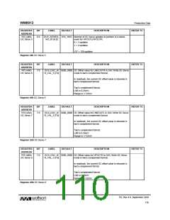
R104 (68h)
Class W 0
0
CP_DYN_PWR
0
Enable dynamic charge pump power control
0 = Charge pump controlled by volume register settings
(Class G)
1 = Charge pump controlled by real-time audio level
(Class W)
Class W is recommended for lowest power
consumption.
Register 68h Class W 0
REGISTER
ADDRESS
BIT
LABEL
DEFAULT
DESCRIPTION
REFER TO
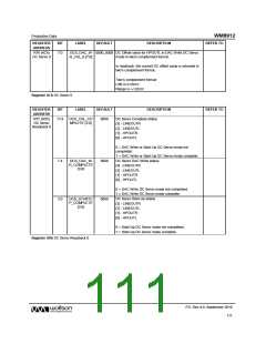
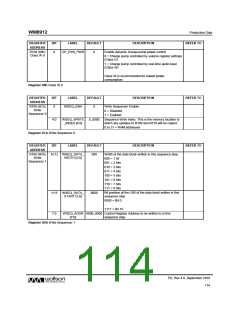
R108 (6Ch)
Write
Sequencer 0
8
WSEQ_ENA
0
Write Sequencer Enable.
0 = Disabled
1 = Enabled
4:0
WSEQ_WRITE
_INDEX [4:0]
0_0000
Sequence Write Index. This is the memory location to
which any updates to R109 and R110 will be copied.
0 to 31 = RAM addresses
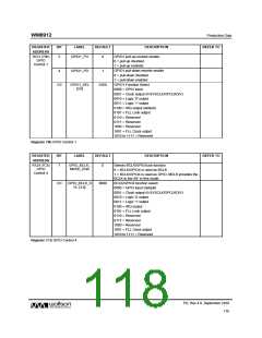
Register 6Ch Write Sequencer 0
REGISTER
ADDRESS
BIT
LABEL
DEFAULT
DESCRIPTION
REFER TO
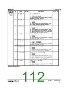
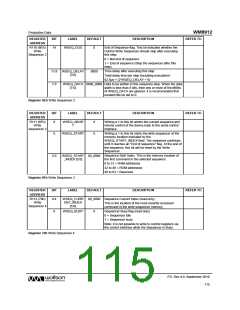
R109 (6Dh) 14:12 WSEQ_DATA_
000
Width of the data block written in this sequence step.
Write
Sequencer 1
WIDTH [2:0]
000 = 1 bit
001 = 2 bits
010 = 3 bits
011 = 4 bits
100 = 5 bits
101 = 6 bits
110 = 7 bits
111 = 8 bits
11:8
7:0
WSEQ_DATA_
START [3:0]
0000
Bit position of the LSB of the data block written in this
sequence step.
0000 = Bit 0
…
1111 = Bit 15
WSEQ_ADDR 0000_0000 Control Register Address to be written to in this
[7:0]
sequence step.
Register 6Dh Write Sequencer 1
PD, Rev 4.0, September 2010
114
w

 WOLFSON [ WOLFSON MICROELECTRONICS PLC ]