WM8912
Production Data
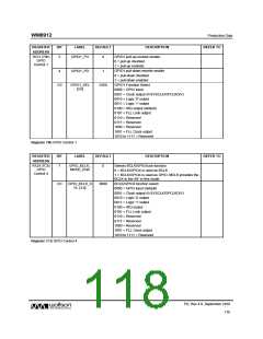
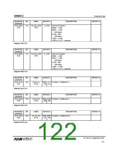
REGISTER
ADDRESS
BIT
LABEL
DEFAULT
DESCRIPTION
GPIO1 pull-up resistor enable
REFER TO
R121 (79h)
GPIO
Control 1
5
GPIO1_PU
0
0 = pull-up disabled
1 = pull-up enabled
4
GPIO1_PD
1
GPIO1 pull-down resistor enable
0 = pull-down disabled
1 = pull-down enabled
GPIO1 Function Select
0000 = GPIO input
3:0
GPIO1_SEL
[3:0]
0100
0001 = Clock output (f=SYSCLK/OPCLKDIV)
0010 = Logic '0' output
0011 = Logic '1' output
0100 = IRQ output (default)
0101 = FLL Lock output
0110 = Reserved
0111 = Reserved
1000 = Reserved
1001 = FLL Clock output
1010 to 1111 = Reserved
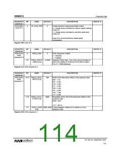
Register 79h GPIO Control 1
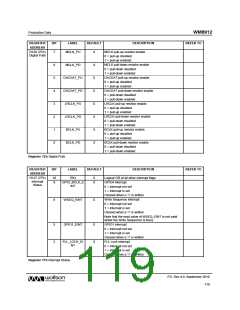
REGISTER
ADDRESS
BIT
LABEL
DEFAULT
DESCRIPTION
REFER TO
R124 (7Ch)
GPIO
Control 4
7
GPIO_BCLK_
MODE_ENA
0
Selects BCLK/GPIO4 pin function
0 = BCLK/GPIO4 is used as BCLK
1 = BCLK/GPIO4 is used as GPIO. MCLK provides the
BCLK in the AIF in this mode.
3:0
GPIO_BCLK_S
EL [3:0]
0000
BCLK/GPIO4 function select:
0000 = GPIO input (default)
0001 = Clock output (f=SYSCLK/OPCLKDIV)
0010 = Logic '0' output
0011 = Logic '1' output
0100 = IRQ output
0101 = FLL Lock output
0110 = Reserved
0111 = Reserved
1000 = Reserved
1001 = FLL Clock output
1010 to 1111 = Reserved
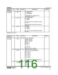
Register 7Ch GPIO Control 4
PD, Rev 4.0, September 2010
118
w

 WOLFSON [ WOLFSON MICROELECTRONICS PLC ]