WM8805
Production Data
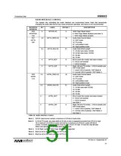
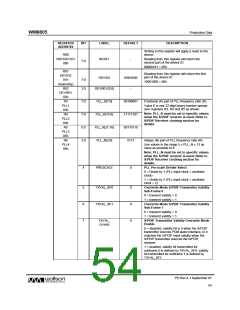
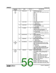
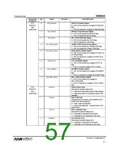
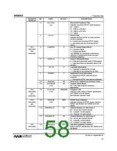
REGISTER
ADDRESS
BIT
LABEL
DEFAULT
DESCRIPTION
Writing to this register will apply a reset to the
device.
R00
RST/DEVID1
00h
RESET
-
Reading from this register will return the
second part of the device ID
7:0
00000101 = 05h
R01
DEVID2
01h
Reading from this register will return the first
part of the device ID
DEVID2
10001000
-
7:0
3:0
10001000 = 88h
(read only)
R02
DEVREV[3:0]
DEVREV
02h
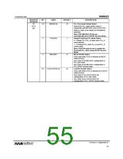
R3
7:0
7:0
5:0
3:0
PLL_K[7:0]
PLL_K[15:8]
PLL_K[21:16]
PLL_N[3:0]
00100001
11111101
00110110
0111
Fractional (K) part of PLL frequency ratio (R).
PLL1
03h
Value K is one 22-digit binary number spread
over registers R3, R4 and R5 as shown.
Note: PLL_K must be set to specific values
when the S/PDIF receiver is used. Refer to
S/PDIF Receiver clocking section for
details.
R4
PLL2
04h
R5
PLL3
05h
R6
Integer (N) part of PLL frequency ratio (R).
PLL4
06h
Use values in the range 5 ≤ PLL_N ≤ 13 as
close as possible to 8
Note: PLL_N must be set to specific values
when the S/PDIF receiver is used. Refer to
S/PDIF Receiver clocking section for
details.
4
PRESCALE
0
PLL Pre-scale Divider Select
0 = Divide by 1 (PLL input clock = oscillator
clock)
1 = Divide by 2 (PLL input clock = oscillator
clock ÷ 2)
5
6
7
TXVAL_SF0
TXVAL_SF1
0
0
0
Overwrite Mode S/PDIF Transmitter Validity
Sub-Frame 0
0 = transmit validity = 0
1 = transmit validity = 1
Overwrite Mode S/PDIF Transmitter Validity
Sub-Frame 1
0 = transmit validity = 0
1 = transmit validity = 1
TXVAL_
OVWR
S/PDIF Transmitter Validity Overwrite Mode
Enable
0 = disabled, validity bit is 0 when the S/PDIF
transmitter sources PCM audio interface, or it
matches the S/PDIF input validity when the
S/PDIF transmitter sources the S/PDIF
receiver.
1 = enabled, validity bit transmitted for
subframe 0 is defined by TXVAL_SF0, validity
bit transmitted for subframe 1 is defined by
TXVAL_SF1.
PD Rev 4.1 September 07
54
w

 WOLFSON [ WOLFSON MICROELECTRONICS PLC ]