WM8805
Production Data
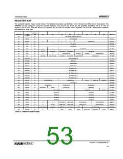
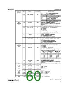
REGISTER
ADDRESS
BIT
LABEL
DEFAULT
DESCRIPTION
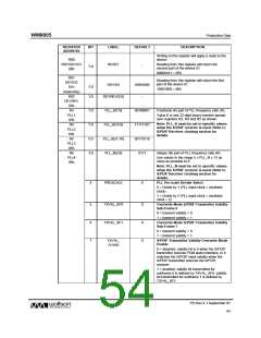
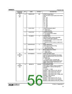
S/PDIF Rx Input Select
R8
PLL6
08h
2:0
RXINSEL[2:0]
000
Select the S/PDIF input to pass to the receiver
circuit.
000 – RX0
001 – RX1
010 – RX2
011 – RX3
100 – RX4
101 – RX5
110 – RX6
111 – RX7
3
4
5
CLKOUTSRC
CLKOUTDIS
FILLMODE
1
1
0
CLKOUT Pin Source Select
0 = Select CLK1
1 = Select OSCCLK
CLKOUT Pin Disable
0 = Pin Disabled (Pin tri-stated)
1 = Pin Enabled
Fill Mode Select
Determines S/PDIF receiver action when
corrupt or invalid data is detected:
0 = Data from S/PDIF receiver remains static
at last valid sample.
1 = Data from S/PDIF receiver is output as all
zeros.
6
ALWAYSVALID
0
Always Valid Select
Used to ignore the INVALID flag.
0 = Use INVALID flag.
1 = Ignore INVALID flag.
MCLK Output Source Select
0 = Select CLK2
7
MCLKSRC
0
1 = Select OSCCLK
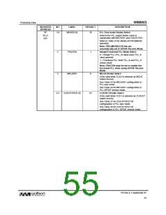
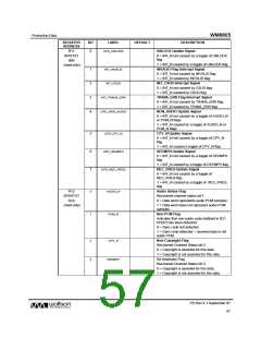
R9
SPDMODE
09h
7:0
SPDIFINMODE
11111111
S/PDIF Input Mode Select
Selects the input circuit type for the receiver
input. The LSB represents RX0 and the MSB
represents RX7
0 = CMOS input
1 = Comparator input. Compatible with
500mVppAC coupled consumer S/PDIF input
signals. Refer to S/PDIF specification (IEC
60958-3) for full details.
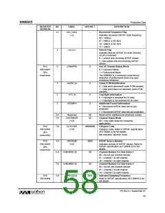
R10
INTMASK
0Ah
7:0
MASK[7:0]
00000000
Interrupt Mask Enable
When a flag is masked, it does not update the
Error Register or cause an interrupt to be
asserted.
0 = unmask, 1 = mask.
MASK[0] = mask control for UPD_UNLOCK
MASK[1] = mask control for INT_INVALID
MASK[2] = mask control for INT_CSUD
MASK[3] = mask control for INT_TRANS_ERR
MASK[4] = mask control for
UPD_NON_AUDIO
MASK[5] = mask control for UPD_CPY_N
MASK[6] = mask control for UPD_DEEMPH
MASK[7] = mask control for UPD_REC_FREQ
PD Rev 4.1 September 07
56
w

 WOLFSON [ WOLFSON MICROELECTRONICS PLC ]