Production Data
WM8352
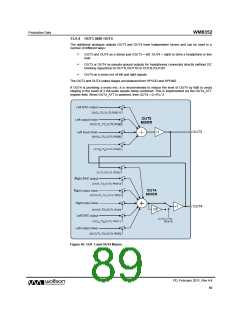
13.10 DIGITAL AUDIO INTERFACE
The audio interface enables the WM8352 to exchange audio data with other system components. It
is separate from the control interface and has four dedicated pins:
.
.
.
.
ADCDAT: Output pin for data coming from the audio ADC
DACDAT: Input pin for audio data going to the audio DAC
LRCLK: Data Left/Right alignment clock (also known as “word clock”)
BCLK: Bit clock, for synchronisation
The LRCLK and BCLK pins are outputs when the WM8352 operates as a master device and are
inputs when it is a slave device.
In order to allow the ADC and DAC to run at different sampling rates, separate ADCLRCLK and
ADCBCLK signals are both available through GPIO pins: GPIO5 (ADCLRCLK) and GPIO6 or GPIO8
(ADCBCLK). This feature also allows mixed Master/Slave operation between the ADC and DAC.
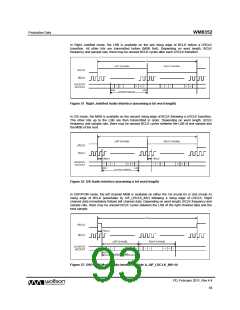
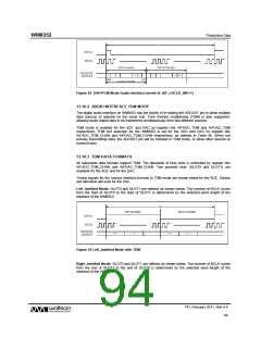
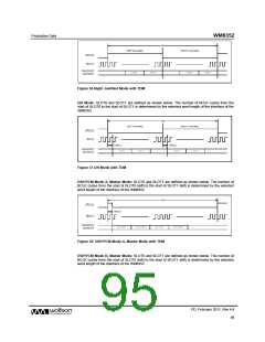
13.10.1 AUDIO DATA FORMATS
The audio interface supports six different audio data formats:
.
.
.
.
.
.
Left justified
Right justified
I2S
DSP mode A
DSP mode B
TDM Mode
In all of these formats, the MSB (most significant bit) of each data sample is transferred first and the
LSB (least significant bit) last.
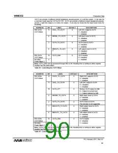
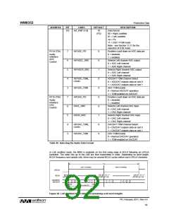
ADDRESS
BIT
LABEL
DEFAULT
DESCRIPTION
BCLK polarity
R112 (70h)
15
AIF_BCLK_INV
0
Audio
0 = normal
Interface
1 = inverted
13
12
AIF_TRI
0
0
Sets Output enables for LRCLK and
BCLK and ADCDAT to inactive state
0 = normal
1 = forces pins to Hi-Z
LRCLK clock polarity
0 = normal
AIF_LRCLK_IN
V
1 = inverted
DSP Mode – mode A/B select
0 = MSB is available on 2nd BCLK rising
edge after LRCLK rising edge (mode A)
1 = MSB is available on 1st BCLK rising
edge after LRCLK rising edge (mode B)
11:10 AIF_WL [1:0]
10
Data word length
11 = 32 bits
10 = 24 bits
01 = 20 bits
00 = 16 bits
(24 bits)
Note: When using the Right-Justified
data format (AIF_FMT=00), the
maximum word length is 24 bits.
PD, February 2011, Rev 4.4
91
w

 WOLFSON [ WOLFSON MICROELECTRONICS PLC ]