Production Data
WM8352
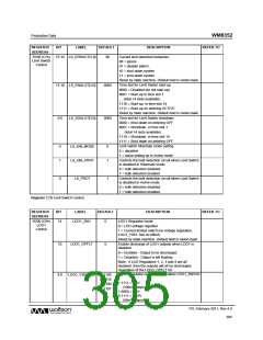
REGISTER
ADDRESS
BIT
6:0
LABEL
DEFAULT
DESCRIPTION
REFER TO
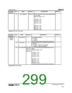
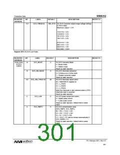
DC4_VIMG[6:0]
000_0110 DC-DC4 Converter output image voltage settings
in 25mv steps.
Maximum output = 3.4V.
110 0110 = 3.4V
110 0010 = 3.3V
101 0110 = 3.0V
100 1110 = 2.8V
……
010 0110 = 1.8V
000 1110 = 1.2V
000 0110 = 1.0V
000 0000 = 0.85V
Register BFh DCDC4 Low Power
REGISTER
ADDRESS
BIT
LABEL
DEFAULT
DESCRIPTION
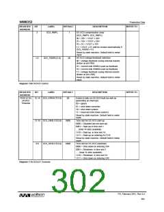
DC-DC5 Converter Mode
REFER TO
R192 (C0h)
DCDC5
Control
14
DC5_MODE
0
0 = Boost mode
1 = Switch mode
Reset by state machine.
DC-DC5 Hibernate behaviour:
0 = Continue as in Active state
1 = Disable converter output
Reset by state machine.
DC-DC5 Hibernate signal select
00 = HIBERNATE register bit
01 = L_PWR1
12
DC5_HIB_MODE
0
9:8
DC5_HIB_TRIG[1:0]
00
10 = L_PWR2
11 = L_PWR3
Note that Hibernate is also selected when a GPIO
Hibernate input is asserted.
Reset by state machine.
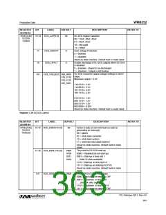
DC-DC5 peak current limit select
0 = Higher peak current
1 = Lower peak current
6
4
DC5_ILIM
0
0
Reset by state machine. Default held in metal
mask.
DC5_RMPH
DC-DC5 compensation ramp
{DC5_RMPH, DC5_RMPL}
00 = 20V < VOUT ≤ 30V
01 = 10V < VOUT ≤ 20V
10 = 5V < VOUT ≤ 10V
11 = VOUT ≤ 5V (will be chosen automatically if
DC5_FBSRC=11)
Reset by state machine. Default held in metal
mask.
PD, February 2011, Rev 4.4
301
w

 WOLFSON [ WOLFSON MICROELECTRONICS PLC ]