Production Data
WM8352
REGISTER
ADDRESS
BIT
LABEL
DEFAULT
DESCRIPTION
REFER TO
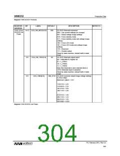
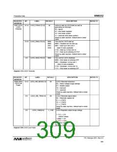
R199 (C7h)
Limit Switch
Control
15:14 LS_ERRACT[1:0]
00
Current limit detection behaviour
00 = ignore
01 = disable switch
10 = shut down system
11 = shut down system
Reset by state machine. Default held in metal mask.
Time slot for Limit Switch start-up
0000 = Disabled (do not start up)
0001 = Start-up in time slot 1
… (total 14 slots available)
13:10 LS_ENSLOT[3:0]
0000
1110 = Start-up in time slot 14
1111 = Start-up on entering ACTIVE
Reset by state machine. Default held in metal mask.
Time slot for Limit Switch shutdown.
0000 = Shut down on entering OFF
0001 = Shutdown in time slot 1
…. (total 14 slots available)
9:6
LS_SDSLOT[3:0]
0000
1110 = Shutdown in time slot 14
1111 = Shut down on entering OFF
Limit switch hibernate mode setting
0 = disabled
4
1
LS_HIB_MODE
LS_HIB_PROT
0
1
1 = leave setting as in Active mode
Controls the bulk detection circuit when Limit Switch
is disabled in Hibernate mode.
0 = bulk detection disabled
1 = bulk detection enabled
0
LS_PROT
1
Controls the bulk detection circuit when Limit Switch
is disabled in Active mode.
0 = bulk detection disabled
1 = bulk detection enabled
Register C7h Limit Switch Control
REGISTER
ADDRESS
BIT
LABEL
DEFAULT
DESCRIPTION
REFER TO
R200 (C8h)
LDO1
Control
14
LDO1_SWI
0
LDO1 Regulator mode
0 = LDO voltage regulator
1 = Current-limited switch (no voltage regulation,
LDO1_VSEL has no effect)
Reset by state machine. Default held in metal mask.
10
LDO1_OPFLT
0
Enable discharge of LDO1 outputs when LDO1 is
disabled
0 = Enabled - Output to be discharged
1 = Disabled - Output is left floating
Note - if LDO Regulators 1, 2, 3 and 4 are all
disabled, then the outputs will all be discharged,
regardless of the LDOn_OPFLT bit.
LDO1 Regulator output voltage (when LDO1_SWI=0)
4:0
LDO1_VSEL[4:0] 1_1100
0_0010
1_1100
1_1101
1 1111 = 3.3V
… (100mV steps)
1 0000 = 1.8V
0 1111 = 1.65V
… (50mV steps)
PD, February 2011, Rev 4.4
305
w

 WOLFSON [ WOLFSON MICROELECTRONICS PLC ]