WM8352
Production Data
REGISTER
ADDRESS
BIT
LABEL
DEFAULT
DESCRIPTION
REFER TO
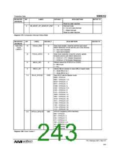
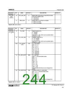
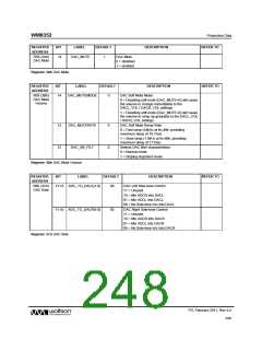
R41 (29h)
Clock
15
LRC_ADC_SEL
0
Selects either ADCLRCLK or DACLRCLK to drive
LRCLK pin in Master mode
Control 2
0 = DACLRCLK
1 = ADCLRCLK
0
MCLK_DIR
0
Whether MCLK is an input or an output.
0 = MCLK is an input
1 = MCLK is an output
Register 29h Clock Control 2
REGISTER
ADDRESS
BIT
LABEL
DEFAULT
DESCRIPTION
REFER TO
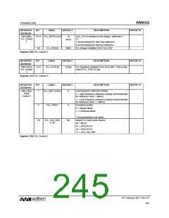
R42 (2Ah)
FLL Control
1
15
FLL_ENA
0
Digital Enable for FLL
0 = disabled
1 = enabled
Note that FLL_OSC_ENA must be enabled before
enabling FLL_ENA.
14
FLL_OSC_ENA
0
Analogue Enable for FLL
0 = FLL disabled
1 = FLL enabled
Note that FLL_OSC_ENA must be enabled before
enabling FLL_ENA.
10:8
FLL_OUTDIV
[2:0]
010
FOUT clock divider
000 = FVCO / 2
001 = FVCO / 4
010 = FVCO / 8
011 = FVCO / 16
100 = FVCO / 32
101 = Reserved
110 = Reserved
111 = Reserved
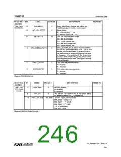
FLL Loop Gain
0000 = x 1 (Recommended value)
0001 = x 2
7:4
FLL_RSP_RATE
0000
0010 = x 4
0011 = x 8
0100 = x 16
0101 = x 32
0110 = x 64
0111 = x 128
1000 = x 256
Recommended that these are not changed from
default.
2:0
FLL_RATE [2:0]
000
Frequency of the FLL control block
000 = FVCO / 1 (Recommended value)
001 = FVCO / 2
010 = FVCO / 4
011 = FVCO / 8
100 = FVCO / 16
101 = FVCO / 32
Recommended that these are not changed from
default.
Register 2Ah FLL Control 1
PD, February 2011, Rev 4.4
244
w

 WOLFSON [ WOLFSON MICROELECTRONICS PLC ]