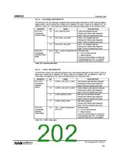
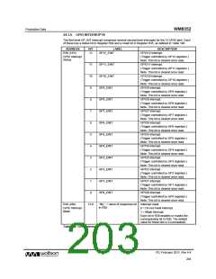
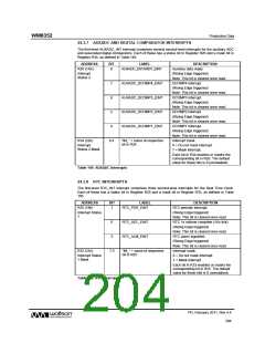
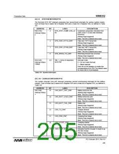
WM8352
Production Data
DESCRIPTION
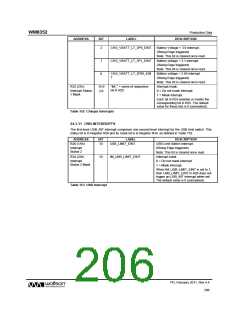
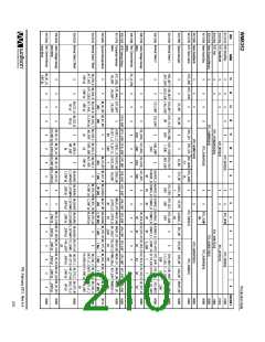
ADDRESS
BIT
LABEL
2
CHG_VBATT_LT_3P9_EINT
Battery Voltage < 3.9 interrupt.
(Rising Edge triggered)
Note: This bit is cleared once read.
Battery voltage < 3.1 interrupt.
(Rising Edge triggered)
1
0
CHG_VBATT_LT_3P1_EINT
Note: This bit is cleared once read.
Battery voltage < 2.85 interrupt.
(Rising Edge triggered)
CHG_VBATT_LT_2P85_EIN
T
Note: This bit is cleared once read.
Interrupt mask.
R33 (21h)
15:9
2:0
“IM_” + name of respective
bit in R25
Interrupt Status
1 Mask
0 = Do not mask interrupt.
1 = Mask interrupt.
Each bit in R33 enables or masks the
corresponding bit in R25. The default
value for these bits is 0 (unmasked).
Table 152 Charger Interrupts
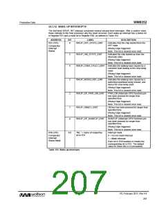
24.3.11 USB INTERRUPTS
The first-level USB_INT interrupt comprises one second-level interrupt for the USB limit switch. This
status bit is in Register R26 and its mask bit is in Register R34, as defined in Table 153.
ADDRESS
BIT
LABEL
DESCRIPTION
USB Limit Switch interrupt.
(Rising Edge triggered)
Note: This bit is cleared once read.
Interrupt mask.
R26 (1Ah)
10
USB_LIMIT_EINT
Interrupt
Status 2
R34 (22h)
10
IM_USB_LIMIT_EINT
Interrupt
Status 2 Mask
0 = Do not mask interrupt.
1 = Mask interrupt.
When IM_USB_LIMIT_EINT is set to 1,
then USB_LIMIT_EINT in R26 does not
trigger an USB_INT interrupt when set.
The default value is 0 (unmasked).
Table 153 USB Interrupt
PD, February 2011, Rev 4.4
206
w

 WOLFSON [ WOLFSON MICROELECTRONICS PLC ]