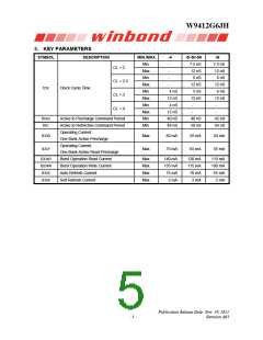
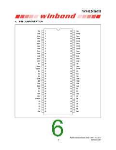
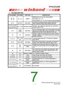
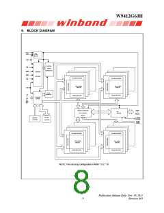
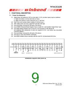
W9412G6JH
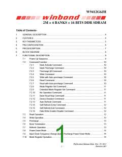
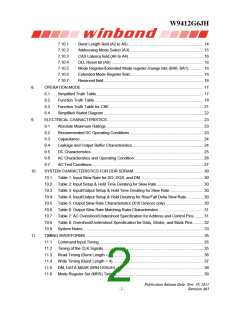
1. GENERAL DESCRIPTION
W9412G6JH is a CMOS Double Data Rate synchronous dynamic random access memory (DDR
SDRAM); organized as 2M words 4 banks 16 bits. W9412G6JH delivers a data bandwidth of up to
500M words per second (-4). To fully comply with the personal computer industrial standard,
W9412G6JH is sorted into the following speed grades: -4, -5, -5I, -5K and -6I. The -4 is compliant to
the DDR500/CL3 and CL4 specification. The -5/-5I/-5K grade parts are compliant to the DDR400/CL3
specification (the -5I industrial grade parts is guaranteed to support -40°C ≤ TA ≤ 85°C, the -5K
automotive grade parts is guaranteed to support -40°C ≤ TA ≤ 105°C). The -6I grade parts is compliant
to the DDR333/CL2.5 specification which is guaranteed to support -40°C ≤ TA ≤ 85°C.
All Input reference to the positive edge of CLK (except for DQ, DM and CKE). The timing reference
point for the differential clock is when the CLK and CLK signals cross during a transition. Write and
Read data are synchronized with the both edges of DQS (Data Strobe).
By having a programmable Mode Register, the system can change burst length, latency cycle,
interleave or sequential burst to maximize its performance. W9412G6JH is ideal for main memory in
high performance applications.
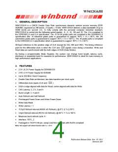
2. FEATURES
2.5V 0.2V Power Supply for DDR400/333
2.4V~2.7V Power Supply for DDR500
Up to 250 MHz Clock Frequency
Double Data Rate architecture; two data transfers per clock cycle
Differential clock inputs (CLK and CLK )
DQS is edge-aligned with data for Read; center-aligned with data for Write
CAS Latency: 2, 2.5, 3 and 4
Burst Length: 2, 4 and 8
Auto Refresh and Self Refresh
Precharged Power Down and Active Power Down
Write Data Mask
Write Latency = 1
15.6µS Refresh interval (4K/64 mS Refresh), @ 0°C ≤ TA ≤ 85°C
3.9µS Refresh interval (4K/16 mS Refresh), @ 85°C < TA ≤ 105°C
Maximum burst refresh cycle: 8
Interface: SSTL_2
Packaged in TSOP II 66-pin, using Lead free materials with RoHS compliant
Note: Not support self refresh function with TA > 85°C
Publication Release Date: Nov. 29, 2011
Revision A03
- 4 -

 WINBOND [ WINBOND ]