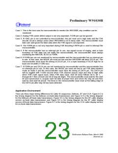
Preliminary W91030B
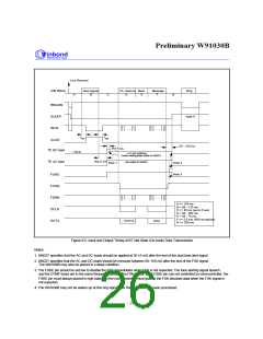
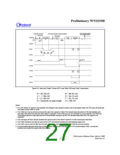
Line Reversal
First Ring Cycle
A/B Wires
Ring Burst
A
Ch. Seizure Mark
Message
B
C
D
E
F
RNGON
SLEEP
Note 4
INTN
...
...
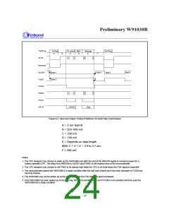
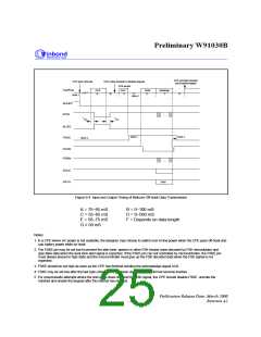
50 - 150 mS
TE DC load
250 - 400 mS
TE AC load
Note 2
Note 3
FSKE
FCDN
FDRN
DCLK
DATA
Note 1
...
...
A = 200 - 450 mS
B >= 500 mS
C = 80 - 262 mS
D = 45 - 262 mS
E <= 2.5 sec (500 mS typical)
F >= 200 mS
...101010...
Data
Figure 9-7. Input and Output Timing of CCA Caller Display Service Data Transmission
Notes:
1. The CPE designer may choose to set FSKE always high while the the CPE is on-hook and the FSK signal is expected.
2. TW/P & E/312 specifies that the AC and DC loads should be applied between 250 400 mS after the end of the ring burst.
-
3. TW/P & E/312 specifies that the AC and DC loads should be removed between 50 150 mS after the end of the FSK signal.
-
The W91030B may also be placed in a sleep condition.
4. The W91030B may not be woken up at the first ring cycle after the FSK data had been processed.
- 28 -

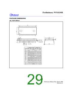
 WINBOND [ WINBOND ]
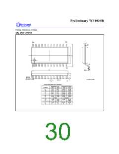