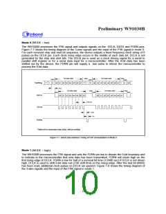
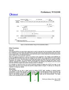
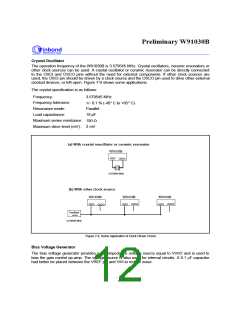
Preliminary W91030B
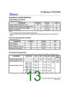
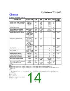
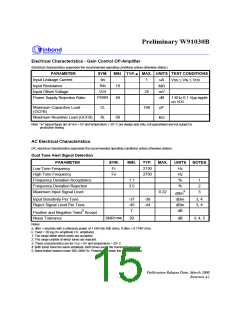
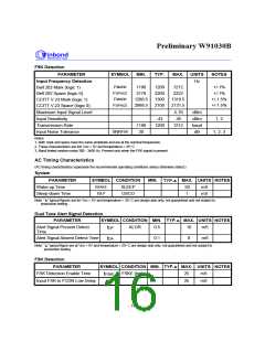
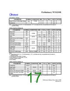
DC Electrical Characteristics, continued
PARAMETER
CONDITION
SYM.
MIN.
MAX. UNITS TEST/
NOTES
TYP§
T+
V
Schmitt Input High Threshold
Schmitt Input Low Threshold
RNGDI,
RNGRC
0.48
0.68
V
V
DD
DD
V
V
SLEEP
0.28
0.48
T-
V
DD
DD
V
V
HYS
Schmitt Hysteresis
V
0.2
V
V
IH
V
DD
DD
CMOS Input High Voltage
CMOS Input Low Voltage
Output High Source Current
DCLK, MODE,
FSKE
0.7 V
V
IL
V
SS
DD
0.3 V
V
Note 1
Note 2
OH
RGNON,
DCLK, DATA,
FDRN, FCDN,
ALGO,
I
0.5
mA
ALGRC, ALGR
OL
Output Low Sink Current
RGNON,
DCLK, DATA,
FDRN, FCDN,
ALGO,
ALGRC,
ALGR, INTN
I
0.5
2.5
mA
Note 2
OL
RNGRC
I
mA
Note 3, 5
IN
Input Current 1
Input Current 2
INP, INN,
RNGDI
I 1
m
A
1
Note 3, 5
IN
SLEEP, DCLK, I 2
MODE, FSKE
10
m
A
Note
4, 5
OZ
Output High-Z Current 1
Output High-Z Current 2
Output High-Z Current 3
Reference Output Voltage
RNGRC
ALGRC
INTN
I
1
2
3
1
5
m
A
OZ
OZ
I
m
A
I
10
m
A
Note 6
Ref
V
DD
DD
0.5 V
+4%
VREF
0.5 V
-4%
V
Ref
R
Reference Output Resistance
VREF
2
W
K
CPth
V
DD
DD
Comparator Threshold
Voltage
ALGRC
0.5 V
-4%
0.5 V
+4%
V
Tests:
1: All input pins are VDD or VSS except for oscillator pins, no analog inputs, output unloaded and SLEEP = VDD.
2: All input pins are VDD or VSS except for oscillator pins, no analog inputs, output unloaded, SLEEP = VSS and FSKE = VDD or
FSKE = VSS.
Notes:
DD
"
" Typical figure are at V = 5V and temperature = 25 C are design aids only, not guaranteed and not subject to production
§
°
testing.
1. VOH = 0.9 VDD.
2. VOL = 0.1 VDD.
3. VIN = VDD to VSS.
4. VOUT = VDD to VSS.
5. Magnitude measurement, ignore signs.
6. Output - no load.
- 14 -

 WINBOND [ WINBOND ]