W90N745CD/W90N745CDG
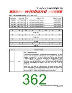
Data Transmit Register 0/1/2/3 (Tx0/1/2/3)
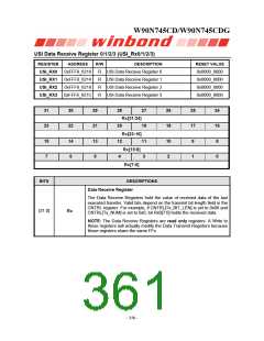
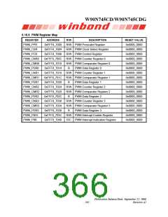
REGISTER
USI_TX0
USI_TX1
USI_TX2
USI_TX3
ADDRESS
R/W
W
DESCRIPTION
USI Data Transmit Register 0
USI Data Transmit Register 1
USI Data Transmit Register 2
USI Data Transmit Register 3
RESET VALUE
0x0000_0000
0x0000_0000
0x0000_0000
0x0000_0000
0xFFF8_6210
0xFFF8_6214
0xFFF8_6218
0xFFF8_621C
W
W
W
31
23
15
7
30
22
14
6
29
28
20
12
4
27
19
11
3
26
18
10
2
25
17
9
24
16
8
Tx[31:24]
21
13
5
Tx[23:16]
Tx[15:8]
Tx[7:0]
1
0
BITS
DESCRIPTIONS
Data Transmit Register
The Data Transmit Registers hold the data to be transmitted in the next
transfer. Valid bits depend on the transmit bit length field in the CNTRL
register. For example, if CNTRL[Tx_BIT_LEN] is set to 0x08 and the
CNTRL[Tx_NUM] is set to 0x0, the bit Tx0[7:0] will be transmitted in next
transfer. If CNTRL[Tx_BIT_LEN] is set to 0x00 and CNTRL[Tx_NUM] is
set to 0x3, the core will perform four 32-bit transmit/receive successive
using the same setting (the order is Tx0[31:0], Tx1[31:0], Tx2[31:0],
Tx3[31:0]).
[31:0]
Tx
NOTE: The RxX and TxX registers share the same flip-flops, which
means that what is received from the input data line in one transfer will
be transmitted on the output data line in the next transfer if no write
access to the TxX register is executed between the transfers.
Publication Release Date: September 22, 2006
- 357 -
Revision A2

 WINBOND [ WINBOND ]