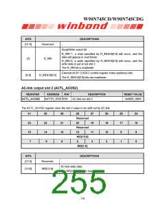
W90N745CD/W90N745CDG
Continued.
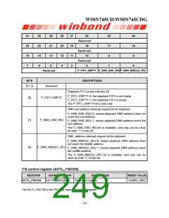
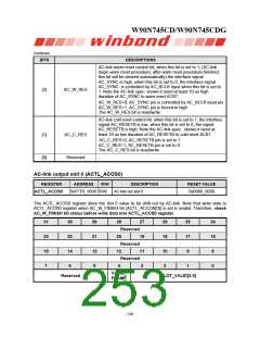
BITS
DESCRIPTIONS
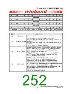
AC-link warm reset control bit, when this bit is set to 1, (AC-link
begin warn reset procedure, after warn reset procedure finished,
this bit will be cleared automatically) the interface signal
AC_SYNC is high, when this bit is set to 0, the interface signal
AC_SYNC is controlled by AC_BCLK input when this bit is set to
1. Note the AC-link spec. shows it need at least 10 us high
duration of AC_SYNC to warn reset AC97.
[2]
AC_W_RES
AC_W_RES=0, AC_SYNC pin is controlled by AC_BCLK input pin
AC_W_RES=1, AC_SYNC pin is forced to high
The AC_W_RES bit is read/write
AC-link cold reset control bit, when this bit is set to 1, the interface
signal AC_RESETB is low, when this bit is set to 0, the signal
AC_RESETB is high. Note the AC-link spec. shows it need at
least 10 us low duration of AC_RESETB to cold reset AC97.
[1]
[0]
AC_C_RES
Reserved
AC_C_RES=0, AC_RESETB pin is set to 1
AC_C_RES=1, AC_RESETB pin is set to 0
The AC_C_RES bit is read/write
-
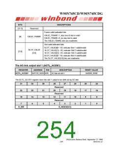
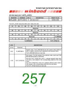
AC-link output slot 0 (ACTL_ACOS0)
REGISTER
ADDRESS
R/W
DESCRIPTION
AC-link out slot 0
RESET VALUE
0xFFF0_9030 R/W
0x0000_0000
ACTL_ACOS0
The ACTL_ACOS0 register store the slot 0 value to be shift out by AC-link. Note that write data to
ACTL_ACOS0 register when AC_W_FINISH bit (ACTL_ACCON[3]) is set is invalid. Therefore, check
AC_W_FINISH bit status before write data into ACTL_ACOS0 register.
31
23
15
7
30
22
14
29
21
13
5
28
Reserved
20
Reserved
12
Reserved
27
19
11
3
26
18
10
2
25
17
9
24
16
8
6
4
1
0
VALID_
FRAME
Reserved
SLOT_VALID[3:0]
- 248 -

 WINBOND [ WINBOND ]