W83759A
Continued
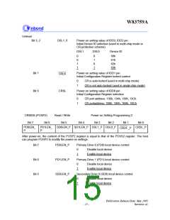
Bit 3, 2
DSL1, 0
Power-on setting value of IDD3, IDD2 pin
Initial Device ID selection (used in multi-chip mode or
CR protection scheme)
DSL1
DSL0
Device ID
0
0
1
1
0
1
0
1
60h
61h
62h
63h
Bit 1
Bit 0
Power-on setting value of IDD1 pin
Initial Configuration Register locked control
CRLK
CRSL
0
1
CR is auto-locked (used in multi-chip mode)
CR is not auto-locked (used in single-chip mode)
Power-on setting value of IDD0 pin
Initial Configuration Register selection
0
1
CR port address: 130h, 134h, 138h, 13Ch
CR portaddress: 1B0h, 1B4h, 1B8h, 1BCh
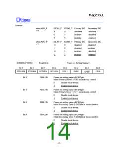
CRX83h (POSP2)
Read / Write
Bit 5
Power-on Setting Programming 2
Bit 7
Bit 6
Bit 4
Bit 3
Bit 2
Bit 1
Bit 0
PD0LEN_
P
PD1LEN_
P
SD0LEN_P SD1LEN_P DSL1_P DSL0_P
CRSL_P
CRLK _P
After power-on, the content of the POSP2 register is equal to that of the POSS2 register. The host
can program POSP2 to modify the power-on settings.
Bit 7
Bit 6
Bit 5
PD0LEN_P
PD1LEN_P
SD0LEN_P
Primary Drive 0 (PD0) local device control
0
1
Disable local device
Enable local device
Primary Drive 1 (PD1) local device control
0
1
Disable local device
Enable local device
Secondary Drive 0 (SD0) local device control
0
1
Disable local device
Enable local device
Publication Release Date: May 1995
Revision A1
- 15 -

 WINBOND [ WINBOND ]