W83759A
CONFIGURATION REGISTERS
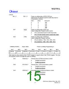
Several configuration registers are implemented in the W83759A. These registers are accessible in
single-chip mode through the index/data port. The index/data port address is 1B4h/1B8h or
134h/138h, depending on whether pin IDD0 is high or low at power-on.
When the W83759A is in multi-chip mode (IDD1 is low at power-on setting), an ID code should be
written to 1B0h/130h (IDIN port). The W83759A will then enter the programming sequence if the ID
code matches the chip ID (determined by IDD2, IDD3 at power-on setting) or leave the programming
sequence if the ID code does not match. After the chip has entered the programming sequence, the
chip ID can be read by reading 1BCh/13Ch (IDOUT port).
IDD0_P is HIGH
1B0h*
IDD0_P is LOW
130h**
IDIN port (W/O)
Index port (R/W)
data port (R/W)
IDOUT port (R/O)
1B4h
134h
1B8h
138h
1BCh
13Ch
* The alias base addresses of 1B0h are XB0h and YB0h, where "X" means 0, 4, 8, C and "Y" means 1, 5, 9, D.
** The alias base addresses of 130h are X30h and Y30h, where "X" means 0, 4, 8, C and "Y" means 1, 5, 9, D.
Index map of configuration registers:
INDEX
Bit 7
Bit 6
Bit 5
Bit 4
Bit 3
Bit 2
Bit 1
Bit 0
Default
Value
8Fh
80h(R/O)
POSS1
81h(R/W)
POSP1
82h(R/O)
POSS2
83h(R/W)
POSP2
84h(R/O)
POSS3
85h(R/W)
POSP3
86h(R/W)
ALTCTL
87h(R/O)
REVID
88h(R/W)
PD0TIM0
89h(R/W)
PD0TIM1
8Ah(R/W)
PD1TIM0
8Bh(R/W)
PD1TIM1
8Ch(R/W)
SD0TIM0
8Dh(R/W)
SD0TIM1
8Eh(R/W)
SD1TIM0
8Fh(R/W)
SD1TIM1
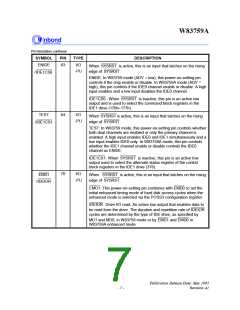
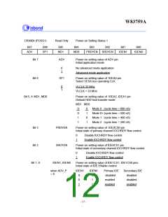
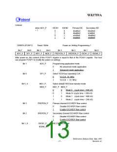
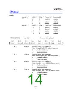
ADV
SP1
MD1
MD0
PRDYEN
PRDYEN_P
DSL1
SRDYEN
SRDYEN_P
DSL0
IDEN1
IDEN0
ADV_P
SP1_P
MD1_P
MD0_P
IDEN1_P
CRLK#
IDEN0_P
CRSL
8Fh
FFh
FFh
FFh
FFh
80h
8Ah
00h
00h
00h
00h
00h
00h
00h
00h
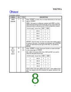
PD0LEN
PD0LE_P
PD0EM#
PD0EM#_P
PD1LEN
PD1LEN_P
PD1EM#
PD1EM#_P
Reserved
Reserved
PD0ACT2
PD0AST0
PD1ACT2
PD1AST0
SD0ACT2
SD0AST0
SD1ACT2
SD1AST0
SD0LEN
SD0LEN_P
SD0EM#
SD0EM#_P
EMD1
SD1LEN
SD1LEN_P
SD1EM#
SD1EM#_P
EMD0
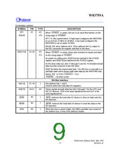
DSL1_P
DSL0_P
CRLK#_P
APD
CRSL_P
SWAP#
SUSPEN
SUSPEN_P
PEMD1_P
Rev 3
STBY#
STBY#_P
PEMD0_P
Rev 2
APD_P
SWAP#_P
SEMD0_P
Rev 0
DMASL#_
P
DMASL#
SEMD1_P
Rev 1
PDRV
SDRV
PD0ACT3
PD0AST1
PD1ACT3
PD1AST1
SD0ACT3
SD0AST1
SD1ACT3
SD1AST1
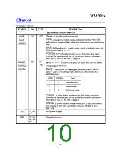
PD0ACT1
PD0DHT1
PD1ACT1
PD1DHT1
SD0ACT1
SD0DHT1
SD1ACT1
SD1DHT1
PD0ACT0
PD0DHT0
PD1ACT0
PD1DHT0
SD0ACT0
SD0DHT0
SD1ACT0
SD1DHT0
PD0RCV3
PD0PRE#
PD1RCV3
PD1PRE#
SD0RCV3
SD0PRE#
SD1RCV3
SD1PRE#
PD0RCV2
PD0DMA#
PD1RCV2
PD1DMA#
SD0RCV2
SD0DMA#
SD1RCV2
SD1DMA#
PD0RCV1
PD0RDY#
PD1RCV1
PD1RDY#
SD0RCV1
SD0RDY#
SD1RCV1
SD1RDY#
PD0RCV0
PD0ADV
PD1RCV0
PD1ADV
SD0RCV0
SD0ADV
SD1RCV0
SD1ADV
Publication Release Date: May 1995
Revision A1
- 11 -

 WINBOND [ WINBOND ]