W83759A
Continued
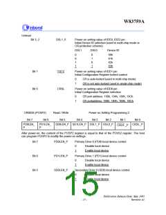
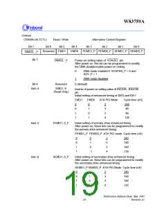
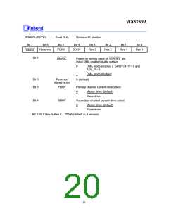
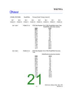
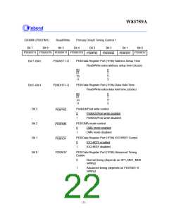
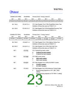
CRX86h (ALTCTL)
Read / Write
Alternative Control Register
Bit 7
Bit 6
Bit 5
Bit 4
Bit 3
Bit 2
Bit 1
Bit 0
Reserved EMD1
EMD0
PEMD1_P PEMD0_P SEMD1_P SEMD0_P
DMASL _P
Bit 7
DMASL _P
Power-on setting value of VGAOEL pin.
After power-on, this bit can be programmed to modify
the DMA disable/enable power-on setting.
0
DMA mode enabled if SUSPEN_P = 0 and
ADV_P = 1
1
DMA mode disabled
Bit 6
Reserved
0 (default)
EMD1, 0
(Read Only)
Bit5- 4
Inverse of power-on setting value of IDEIOR, IDEIOW
pin
Initial setting of enhanced timing of IDE0 and IDE1
EMD1
EMD0
ATA PIO Mode
Cycle time (nS)
0
0
1
1
0
1
0
1
2
3
3
4
240
80
80
120
PEMD1, 0_P
Initial setting of primary drive enhanced timing
After power-on, these bits can be programmed to modify
the primary drive enhanced timing.
Bit3- 2
PEMD1_P PEMD0_P ATA PIO mode Cycle time (nS)
0
0
1
1
0
2
3
3
4
240
180
180
120
1
0
`1
SEMD1, 0_P
Initial setting of secondary drive enhanced timing
After power-on, these bits can be programmed to modify
the secondary drive enhanced timing
Bit1- 0
SEMD1_P SEMD0_P ATA PIO Mode Cycle time (nS)
0
0
1
1
0
1
0
1
2
3
3
4
240
180
180
120
Publication Release Date: May 1995
Revision A1
- 19 -

 WINBOND [ WINBOND ]