W78E54
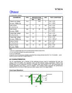
AUXR SFR, which is located at 08Eh. When ALE is turned off, it will be reactivated when the program
accesses external ROM/RAM data or jumps to execute an external ROM code. The ALE signal will
turn off again after it has been completely accessed or the program returns to internal ROM code
space..
The AO bit in the AUXR register, when set, disables the ALE output.
***AUXR - Auxiliary register (8EH)
-
-
-
-
-
-
-
AO
AO: Turn off ALE output.
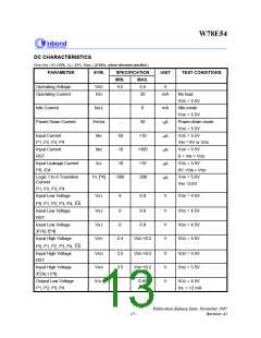
4. Power-off Flag
***PCON - Power control (87H)
-
GF1
GF0
PD
IDL
SMOD
-
POF
SMOD:
POF:
Double baud rate bit. When set to a 1, the baud rate is doubled when the serial port is
being used in either modes 1, 2, 3.
Power off flag. Bit is set by hardware when power on reset. It can be cleared by software
to determine chip reset is a warm boot or cold boot.
GF1, GF0: These two bits are general-purpose flag bits for the user.
PD:
Power down mode bit. Set it to enter power down mode.
Idle mode bit. Set it to enter idle mode.
IDL:
The power-off flag is located at PCON.4. This bit is set when VDD has been applied to the part. It can
be used to determine if a reset is a warm boot or a cold boot if it is subsequently reset by software.
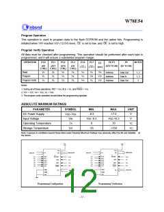
Flash Operations
In normal operation, the W78E54 is functionally compatible with the W78C54. In the flash operating
mode, the flash EEPROM can be programmed and verified repeatedly. Once the code inside the
flash EEPROM is confirmed, the code can be protected. The flash EEPROM and the operations on it
are described below.
All of the operations are configured by the pins RST, ALE, PSEN, A9CTRL (P3.0), A13CTRL (P3.1),
A14CTRL (P3.2), OECTRL (P3.3), CE (P3.6), OE (P3.7), A0 (P1.0) and VPP (EA ). In these
operations, A15 to A0 (P2.7 to P2.0, P1.7 to P1.0) and D7 to D0 (P0.7 to P0.0) serve as the address
and data bus, respectively.
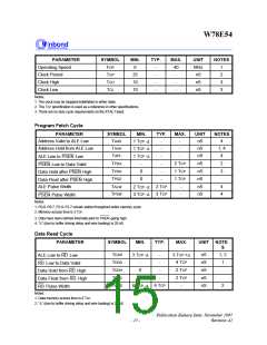
Read Operation
This operation enables customers to read their codes and the option bits. The data will not be valid if
the lock bit is programmed to low.
Publication Release Date: November 1997
- 11 -
Revision A2

 WINBOND [ WINBOND ]