W78E54
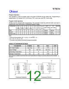
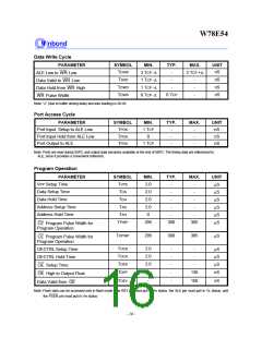
Program Operation
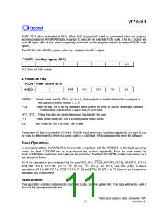
This operation is used to program data to the flash EEPROM and the option bits. Programming is
initiated when VPP reaches VCP (12.5V) level, CE is set to low, and OE is set to high.
Program Verify Operation
All data must be checked after programming. This operation should be performed after each byte is
programmed, and it will ensure a substantial program margin.
OPERATION
P3.0
P3.1
P3.2
P3.3
P3.6
P3.7
P2, P1
P0
NOTES
EA
(A9
CTRL)
(A13
CTRL)
(A14
CTRL)
(OE
CTRL)
(A15 TO A0) (D7 TO D0)
(
)
(
)
OE
CE
(VPP)
Read
VIL
VIL
VIL
VIL
VIL
VIL
VIL
VIL
VIL
VIL
VIL
VIL
VIL
VIL
VIH
VIL
VIH
VIL
VIH
VCP
VCP
Address
Address
Address
Data Out
Data In
1, 2
1, 2
3
Program
Program Verify
Data Out
Notes:
1. During all of these operations, RST = VIH, ALE = VIL, and PSEN = VIH.
2. VCP = 12V, VIH = VDD, VIL = Vss.
3. The program verify operation should follow the programming operaion.
ABSOLUTE MAXIMUM RATINGS
PARAMETER
DC Power Supply
SYMBOL
VDD- VSS
VIN
MIN.
-0.3
MAX.
UNIT
+7.0
VDD +0.3
70
V
V
Input Voltage
VSS -0.3
0
Operating Temperature
Storage Temperature
TA
°C
°C
TST
-55
+150
Note: Exposure to conditions beyond those listed under Absolute Maximum Ratings may adversely affect the life and reliability of
the device.
+5V
+5V
V
V
DD
DD
PGM DATA
PGM DATA
A0 to A7
P1
P0
A0 to A7
P1
P0
V
P3.0
P3.1
P3.2
P3.3
P3.6
P3.7
EA/Vpp
V
P3.0
P3.1
P3.2
P3.3
P3.6
P3.7
EA/Vpp
ALE
IL
IL
IL
IL
IH
IL
IL
IL
IL
IL
IL
IH
V
V
V
V
CP
IL
CP
IL
V
V
V
V
V
V
V
V
V
V
ALE
RST
V
V
RST
V
V
IH
IH
IH
IH
PSEN
PSEN
X'tal1
X'tal2
Vss
X'tal1
X'tal2
Vss
A8 to A15
P2
A8 to A15
P2
Programming Configuration
Programming Verification
- 12 -

 WINBOND [ WINBOND ]