W78E54
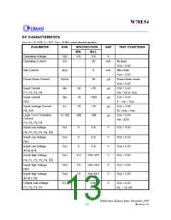
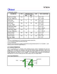
DC Characteristics, continued
PARAMETER
SYM.
SPECIFICATION
UNIT
TEST CONDITIONS
MIN.
MAX.
Output Low Voltage
P0, ALE, PSEN [*3]
VOL2
-
0.45
V
VDD = 4.5V
IOL = +4mA
Sink Current
P1, P2, P3, P4
Sink Current
ISK1
ISK2
4
12
20
mA
mA
VDD = 4.5V
Vs = 0.45V
VDD = 4.5V
Vs = 0.45V
10
P0, ALE, PSEN
Output High Voltage
P1, P2, P3, P4
VOH1
VOH2
2.4
2.4
-
-
V
V
VDD = 4.5V
IOH = -100 mA
VDD = 4.5V
Output High Voltage
IOH = -400 mA
P0, ALE, PSEN [*3]
Source Current
P1, P2, P3, P4
Source Current
ISR1
ISR2
-120
-8
-250
-14
VDD = 4.5V
Vs = 2.4V
VDD = 4.5V
Vs = 2.4V
mA
mA
P0, ALE, PSEN
Notes:
1. RST pin is a Schmitt trigger input. RST has internal pull-low resistors of about 30 KW.
3. P0, ALE and /PSEN are tested in the external access mode.
4. XTAL1 is a CMOS input.
5. Pins of P1, P2, P3, P4 can source a transition current when they are being externally driven from 1 to 0. The transition current
reaches its maximum value when VIN approximates to 2V.
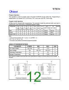
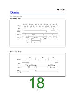
AC CHARACTERISTICS
The AC specifications are a function of the particular process used to manufacture the part, the
ratings of the I/O buffers, the capacitive load, and the internal routing capacitance. Most of the
specifications can be expressed in terms of multiple input clock periods (TCP), and actual parts will
usually experience less than a ±20 nS variation. The numbers below represent the performance
expected from a 0.8 micron CMOS process when using 2 and 4 mA output buffers.
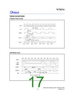
Clock Input Waveform
XTAL1
TCH
TCL
FOP,
TCP
- 14 -

 WINBOND [ WINBOND ]