W25X10BV/20BV/40BV
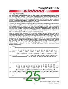
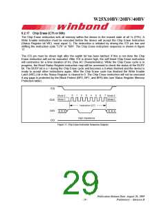
9.2.13 Page Program (02h)
The Page Program instruction allows up to 256 bytes of data to be programmed at previously erased
to all 1s (FFh) memory locations. A Write Enable instruction must be executed before the device will
accept the Page Program Instruction (Status Register bit WEL must equal 1). The instruction is
initiated by driving the /CS pin low then shifting the instruction code “02h” followed by a 24-bit address
(A23-A0) and at least one data byte, into the DIO pin. The /CS pin must be held low for the entire
length of the instruction while data is being sent to the device.
If an entire 256 byte page is to be programmed, the last address byte (the 8 least significant address
bits) should be set to 0. If the last address byte is not zero, and the number of clocks exceed the
remaining page length, the addressing will wrap to the beginning of the page. In some cases, less
than 256 bytes (a partial page) can be programmed without having any effect on other bytes within the
same page. One condition to perform a partial page program is that the number of clocks can not
exceed the remaining page length. If more than 256 bytes are sent to the device the addressing will
wrap to the beginning of the page and overwrite previously sent data.
As with the write and erase instructions, the /CS pin must be driven high after the eighth bit of the last
byte has been latched. If this is not done the Page Program instruction will not be executed. After /CS
is driven high, the self-timed Page Program instruction will commence for a time duration of tpp (See
AC Characteristics). While the Page Program cycle is in progress, the Read Status Register
instruction may still be accessed for checking the status of the BUSY bit. The BUSY bit is a 1 during
the Page Program cycle and becomes a 0 when the cycle is finished and the device is ready to accept
other instructions again. After the Page Program cycle has finished the Write Enable Latch (WEL) bit
in the Status Register is cleared to 0. The Page Program instruction will not be executed if the
addressed page is protected by the Block Protect (BP2, BP1, and BP0) bits (see Status Register
Memory Protection table).
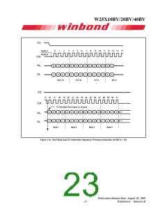
Figure 13. Page Program Instruction Sequence Diagram
Publication Release Date: August 20, 2009
- 25 -
Preliminary -- Revision B

 WINBOND [ WINBOND ]