W25Q16DV
Output (DO) is high impedance, and Serial Data Input (DI) and Serial Clock (CLK) are ignored. The Chip
Select (/CS) signal should be kept active (low) for the full duration of the /HOLD operation to avoid
resetting the internal logic state of the device.
6.2 WRITE PROTECTION
Applications that use non-volatile memory must take into consideration the possibility of noise and other
adverse system conditions that may compromise data integrity. To address this concern, the W25Q16DV
provides several means to protect the data from inadvertent writes.
6.2.1 Write Protect Features
•
•
•
•
•
•
•
Device resets when VCC is below threshold
Time delay write disable after Power-up
Write enable/disable instructions and automatic write disable after erase or program
Software and Hardware (/WP pin) write protection using Status Register
Write Protection using Power-down instruction
Lock Down write protection until next power-up
One Time Program (OTP) write protection*
* Note: This feature is available upon special order. Please contact Winbond for details.
Upon power-up or at power-down, the W25Q16DV will maintain a reset condition while VCC is below the
threshold value of VWI, (See Power-up Timing and Voltage Levels and Figure 39). While reset, all
operations are disabled and no instructions are recognized. During power-up and after the VCC voltage
exceeds VWI, all program and erase related instructions are further disabled for a time delay of tPUW. This
includes the Write Enable, Page Program, Sector Erase, Block Erase, Chip Erase and the Write Status
Register instructions. Note that the chip select pin (/CS) must track the VCC supply level at power-up until
the VCC-min level and tVSL time delay is reached, and it must also track the VCC supply level at power-
down to prevent adverse command sequence. If needed a pull-up resister on /CS can be used to
accomplish this.
After power-up the device is automatically placed in a write-disabled state with the Status Register Write
Enable Latch (WEL) set to a 0. A Write Enable instruction must be issued before a Page Program, Sector
Erase, Block Erase, Chip Erase or Write Status Register instruction will be accepted. After completing a
program, erase or write instruction the Write Enable Latch (WEL) is automatically cleared to a write-
disabled state of 0.
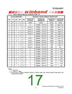
Software controlled write protection is facilitated using the Write Status Register instruction and setting the
Status Register Protect (SRP0, SRP1) and Block Protect (CMP, SEC,TB, BP2, BP1 and BP0) bits. These
settings allow a portion as small as 4KB sector or the entire memory array to be configured as read only.
Used in conjunction with the Write Protect (/WP) pin, changes to the Status Register can be enabled or
disabled under hardware control. See Status Register section for further information. Additionally, the
Power-down instruction offers an extra level of write protection as all instructions are ignored except for
the Release Power-down instruction.
Publication Release Date: October 29, 2012
- 13 -
Revision D

 WINBOND [ WINBOND ]