W25Q16DV
7. STATUS REGISTERS AND INSTRUCTIONS
The Read Status Register-1 and Status Register-2 instructions can be used to provide status on the
availability of the Flash memory array, if the device is write enabled or disabled, the state of write
protection, Quad SPI setting, Security Register lock status and Erase/Program Suspend status. The Write
Status Register instruction can be used to configure the device write protection features, Quad SPI setting
and Security Register OTP lock. Write access to the Status Register is controlled by the state of the non-
volatile Status Register Protect bits (SRP0, SRP1), the Write Enable instruction, and during Standard/Dual
SPI operations, the /WP pin.
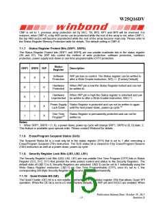
7.1 STATUS REGISTERS
7.1.1 BUSY Status (BUSY)
BUSY is a read only bit in the status register (S0) that is set to a 1 state when the device is executing a
Page Program, Quad Page Program, Sector Erase, Block Erase, Chip Erase, Write Status Register or
Erase/Program Security Register instruction. During this time the device will ignore further instructions
except for the Read Status Register and Erase/Program Suspend instruction (see tW, tPP, tSE, tBE, and
tCE in AC Characteristics). When the program, erase or write status/security register instruction has
completed, the BUSY bit will be cleared to a 0 state indicating the device is ready for further instructions.
7.1.2 Write Enable Latch Status (WEL)
Write Enable Latch (WEL) is a read only bit in the status register (S1) that is set to 1 after executing a
Write Enable Instruction. The WEL status bit is cleared to 0 when the device is write disabled. A write
disable state occurs upon power-up or after any of the following instructions: Write Disable, Page
Program, Quad Page Program, Sector Erase, Block Erase, Chip Erase, Write Status Register, Erase
Security Register and Program Security Register.
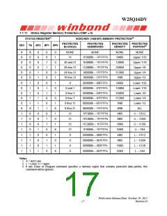
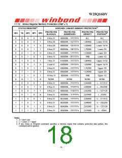
7.1.3 Block Protect Bits (BP2, BP1, BP0)
The Block Protect Bits (BP2, BP1, BP0) are non-volatile read/write bits in the status register (S4, S3, and
S2) that provide Write Protection control and status. Block Protect bits can be set using the Write Status
Register Instruction (see tW in AC characteristics). All, none or a portion of the memory array can be
protected from Program and Erase instructions (see Status Register Memory Protection table). The
factory default setting for the Block Protection Bits is 0, none of the array protected.
7.1.4 Top/Bottom Block Protect Bit (TB)
The non-volatile Top/Bottom bit (TB) controls if the Block Protect Bits (BP2, BP1, BP0) protect from the
Top (TB=0) or the Bottom (TB=1) of the array as shown in the Status Register Memory Protection table.
The factory default setting is TB=0. The TB bit can be set with the Write Status Register Instruction
depending on the state of the SRP0, SRP1 and WEL bits.
7.1.5 Sector/Block Protect Bit (SEC)
The non-volatile Sector/Block Protect bit (SEC) controls if the Block Protect Bits (BP2, BP1, BP0) protect
either 4KB Sectors (SEC=1) or 64KB Blocks (SEC=0) in the Top (TB=0) or the Bottom (TB=1) of the array
as shown in the Status Register Memory Protection table. The default setting is SEC=0.
7.1.6 Complement Protect Bit (CMP)
The Complement Protect bit (CMP) is a non-volatile read/write bit in the status register (S14). It is used in
conjunction with SEC, TB, BP2, BP1 and BP0 bits to provide more flexibility for the array protection. Once
- 14 -

 WINBOND [ WINBOND ]