Preliminary W24100
Timing Waveforms, continued
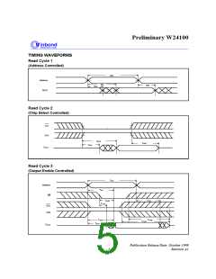
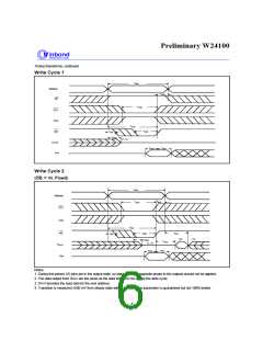
Write Cycle 1
T
WC
Address
OE
T
WR
T
CW
CS1
CS2
T
AW
T
WP
WE
T
AS
T
OHZ
(1, 4)
DOUT
T
T
DH
DW
D
IN
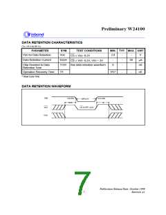
Write Cycle 2
(OE = VIL Fixed)
T
WC
Address
CS1
T
WR
T
CW
CS2
WE
T
AW
T
T
OH
WP
T
AS
(2)
(3)
T
WHZ
T
OW
(1, 4)
D
OUT
T
DH
T
DW
D
IN
Notes:
1. During this period, I/O pins are in the output state, so input signals of opposite phase to the outputs should not be applied.
2. The data output from DOUT are the same as the data written to DIN during the write cycle.
OUT
3. D
provides the read data for the next address.
4. Transition is measured 500 mV from steady state with CL = 5 pF. This parameter is guaranteed but not 100% tested.
±
- 6 -

 WINBOND [ WINBOND ]