Preliminary
VG37648041AT
256M:x4, x8, x16
VIS
CMOS Synchronous Dynamic RAM
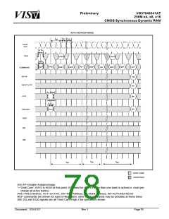
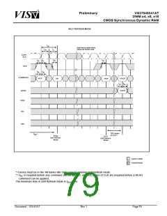
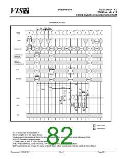
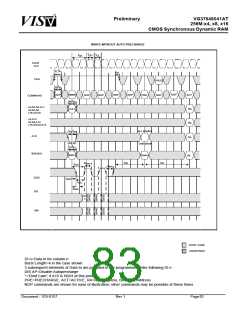
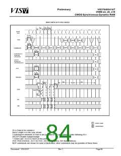
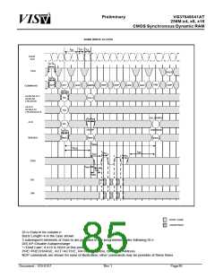
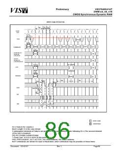
BANK WRITE ACCESS
t
t
t
CH
CL
CK
CLK#
CLK
t
t
IS IH
CKE
VALID
t
t
IS
IH
PRE
NOP
NOP
NOP
ACT
NOP
NOP
WRITE
NOP
NOP
COMMAND
t
t
IH
IS
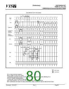
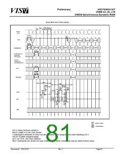
x4:A0,A9,A11
x8:A0,A9
RA
Col n
x16:A0,A8
x4:A12
x8:A9,A12
x16:A8,A9,A12
RA
ALL BANKS
t
t
IS IH
A10
RA
DIS AP
Bank x
t
t
ONE BANK
IH
IS
BA0,BA1
Bank x
*Bank x
t
RAS
t
RCD
tWR
tDSH
tDSS
tWPO
DQS
tWCP
tDSL
tWPR
DQ
DM
Dl
n
DONT’ CARE
UNDEFINED
DI n=Data In for column n
Burst Length=4 in the case shown
3 subsequent elements of Data In are provided in the programmed order following DI n
DIS AP=Disable Autoprecharge
*=”Dont’ Care”, if A10 is HIGH at this point
PRE=PRECHARGE, ACT=ACTIVE, RA=Row Address, BA=Bank Address
NOP commands are shown for ease of illustration; other commands may be possible at these times
Document : 1G5-0157
Rev.1
Page85

 VML [ VANGUARD INTERNATIONAL SEMICONDUCTOR ]