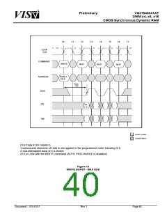
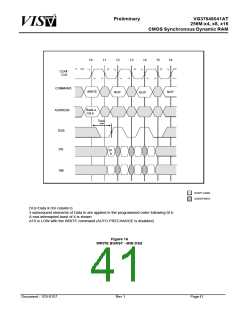
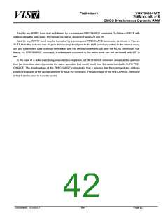
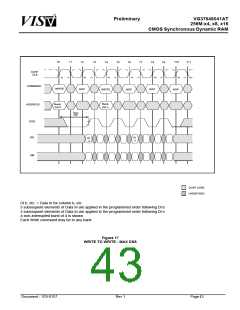
PDF
最近搜索
热门搜索
发布采购

| 型号: | VG37648041AT |
| PDF下载: | 下载PDF文件 查看货源 |
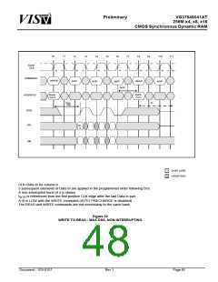
| 内容描述: | 256M : X4,X8 , X16 CMOS同步动态RAM [256M:x4, x8, x16 CMOS Synchronous Dynamic RAM] |
| 分类和应用: | |
| 文件页数/大小: | 86 页 / 964 K |
| 品牌: |  VML [ VANGUARD INTERNATIONAL SEMICONDUCTOR ] VML [ VANGUARD INTERNATIONAL SEMICONDUCTOR ] |
专业IC领域供求交易平台:提供全面的IC Datasheet资料和资讯,Datasheet 1000万数据,IC品牌1000多家。