VSC8601 Datasheet
Electrical Specifications
Table 72.
AC Characteristics for the SMI Interface (continued)
Parameter
Symbol Minimum
Typical
50
Maximum
Unit Condition
MDC time high
MDC time low
tWH
tWL
tSU
tH
20
20
10
10
ns
ns
ns
ns
ns
50
Setup to MDC rising
Hold from MDC rising
MDC rise time
tR
100
For MDC = 0 – 1 MHz
t
CYC × 10%(1)
For MDC = 1 MHz – fCLK(MAX)
MDC fall time
tF
100
tCYC × 10%(1)
300
MDC to MDIO valid
tCO
10
ns
Time dependant on value of
external pull-up resistor on
MDIO pin
1. For fCLK above 1 MHz, the maximum rise time and fall time is in relation to the frequency of the MDC clock
period. For example, if fCLK is 2 MHz, the maximum clock rise time and fall time is 50 ns.
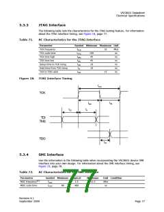
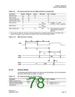
Figure 19.
SMI Interface Timing
tWH
tWL
MDC
tCYC
tSU
tH
MDIO
(write)
Data
tCO
MDIO
(read)
Data
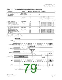
5.3.5
Device Reset
The following specifications apply to the device reset functionality. For more information
about the reset timing, see Figure 20, page 79.
Table 73.
AC Characteristics for Device Reset
Parameter
Symbol
tRESET
tWAIT
Minimum Maximum Unit Condition
NRESET assertion time
100
ns
Wait time between NRESET
de-assert and access of the
SMI interface
20
220
ms Register 21E.14 = 0
ms Register 21E.14 = 1
Revision 4.1
September 2009
Page 78

 VITESSE [ VITESSE SEMICONDUCTOR CORPORATION ]