VSC838-01
Datasheet
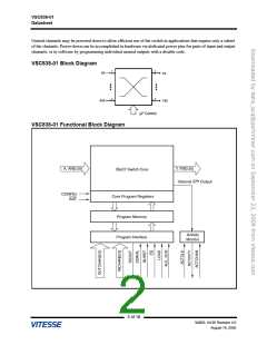
Functional Descriptions
Input/Output Characteristics
All input data must be differential and should be nominally biased to +2.0V or AC-coupled. Other levels are allowed.
For more information, see “Input Terminations,” page 9. On-chip terminations are provided, with a nominal
impedance of 100Ω differential. All input termination resistors float with an internal bias provided for AC-coupling.
For direct interconnection of multiple VSC838-01 devices, a CML termination mode is provided by tying the ITC pin
to V , which ties the center point of the 100Ω termination to V , causing the terminations to act as loads for an
CC
CC
open-drain or open-collector differential output.
Data outputs are provided through differential current switches with on-chip back-termination. The output circuit is
capable of driving external 50Ω far-end termination (recommended). The output back-terminations are electronically
switchable to enable a power savings of 1W (max) by reducing the output driver current.
Programming Interface
Parallel Mode
In parallel mode (SERIAL=0), the binary word on INCHAN[5:0] is the numerical identifier of the input that will be
routed to the specified output. OUTCHAN[5:0] is the numerical identifier of the output being programmed. A rising
edge on the LOAD signal will transfer the programming data to the shadow register in the program memory. Raising
CONFIG (asynchronously) will transfer the programming data to the main latches in the program memory and cause
the internal select signals in the core to re-configure the multiplexer. Lowering CONFIG will latch the main latches.
CONFIG may be tied HIGH to enable programming to take effect instantaneously.
This interface may be used with multiplexed address/data buses by using only INCHAN[5:0] without
OUTCHAN[5:0] and dropping ALE when the address of the output to be programmed is present on INCHAN[5:0].
After the address is latched, the input address may be presented on INCHAN[5:0] and programming proceeds as
above.
No read-back capability is provided in parallel mode. Read-back for diagnostic purposes is provided in serial mode
via the scan function.
Serial Mode
In serial mode (SERIAL=1), the INCHAN[0] pin becomes the serial data input SDIN and the INCHAN[1] pin
becomes the serial clock SCLK (rising edge triggered). A serial word of the form [Output][Input] is shifted into the
internal shift register, and the LOAD pin is asserted (HIGH) coincident with the last bit of the data word to signal that
the word is to be applied. This transfers the input identifier to the shadow register of the addressed output. CONFIG is
then applied (asynchronously) to transfer one or more program commands to the main latches of the program
memories.
The SDOUT pin follows the data on the INCHAN[0](SDIN) pin 14 clock cycles later. This enables the user to chain
the serial ports of several crosspoints, shift program data for all switches through such a chain, and assert LOAD on
all switches to program all of the connections simultaneously.
The output field is 7 bits long, representing the binary numerical identifier of the output to be programmed. The input
field is 7 bits long, representing the numerical identifier of the input that will be routed to the specified output.
3 of 19
VMDS-10195 Revision 4.0
August 19, 2005

 VITESSE [ VITESSE SEMICONDUCTOR CORPORATION ]