VSC838-01
Datasheet
Unused channels may be powered down to allow efficient use of the switch in applications that require only a subset
of the channels. Power-down can be accomplished in hardware via dedicated power pins for pairs of input and output
channels, or in software by programming individual unused outputs with a disable code.
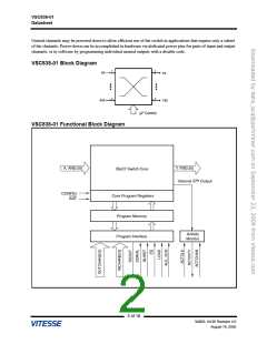
VSC838-01 Block Diagram
2
2
A0
Y0
2
2
A35
Y35
µP Control
VSC838-01 Functional Block Diagram
A, AN[0:35]
Y, YN[0:35]
36x37 Switch Core
Internal 37th Output
CONFIG
INIT
Core Program Registers
Program Memory
Activity
Monitor
Program Interface
2 of 19
VMDS-10195 Revision 4.0
August 19, 2005

 VITESSE [ VITESSE SEMICONDUCTOR CORPORATION ]