VSC7961
Data Sheet
SPECIFICATIONS
Over Recommended Operating Conditions.
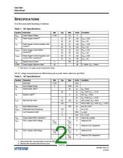
Table 1. DC Specifications
Symbol Parameter
Min
Typ
Max
5.5
37
Units
V
Condition
V
Power Supply Voltage
Power Supply Current
3.135
CC
(1)
I
I
I
I
I
31
35
59
62
23
30
62
67
mA
mA
mA
mA
mA
mA
mA
mA
µA
V
V
V
V
V
V
V
V
= 3.3V
= 5V
EE
CC
CC
CC
CC
CC
CC
CC
CC
43
Power Supply Current Including Load
Current
67
= 3.3V
= 5V
CC
(1)
72
Power Supply Current When
Squelched
30
= 3.3V
= 5V
EESQ
CCSQ
SQ
(1)
35
Power Supply Current Including Load
Current When Squelched
72
= 3.3V
= 5V
(1)
75
Squelch Input Current
0
400
PSRR
Power Supply Rejection Ratio
20
dB
f < 2MHz, V = 100mV
IN
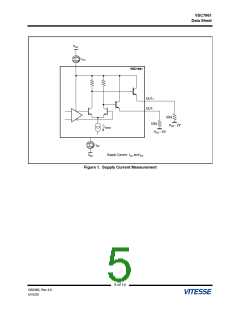
1. See Figure 1 for supply current measurement setup.
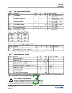
All AC voltage measurements are differential peak-to-peak, unless otherwise specified.
Table 2. AC Specifications
Symbol Parameter
Min
3.125
5
Typ
Max
Units Condition
Data Rate
Gb/s
mV
V
J
Input Voltage Range
1200
35
IN
(1)
Deterministic Jitter
ps
ps
V
V
>10mV.
D
IN
50
= 5mV, V = +3.3V.
CC
IN
(2)
J
t
Random Jitter
9
ps
rms, V > 10mV.
IN
R
11
90
ps
V
= 5mV, V = +3.3V.
IN CC
t
Rise and Fall Times
120
230
ps
20% to 80%, V >10mV.
IN
R,
F
140
ps
20% to 80%, V = 5mV, V = +3.3V.
IN CC
V
Input Referred Noise
µV
Ω
rms, IN+ to IN–.
IN+ to IN–.
C open.
N
R
Differential Input Resistance
Low Frequency Cutoff
100
2
DIFF
f
MHz
kHz
mV
V
L
Z
2
C = 0.1µF.
Z
V
Output Signal When Squelched
PECL Output HIGH Voltage
40
Output AC-coupled.
Tested at 3.3V.
SQ
V
V
–
V
–
CC
OH
CC
0.105
0.85
V
0.85
–
V
V
V
Tested at 3.3V. Squelched.
Tested at 3.3V.
CC
V
PECL Output LOW Voltage
V
–
V
1.47
–
CC
OL
CC
1.81
V
–
Tested at 3.3V. Squelched.
CC
0.95
1. Deterministic jitter measured peak-to-peak with K28.5 pattern.
2. Random jitter measured with minimum input.
2 of 14
G52360, Rev 4.0
5/15/03

 VITESSE [ VITESSE SEMICONDUCTOR CORPORATION ]