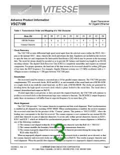
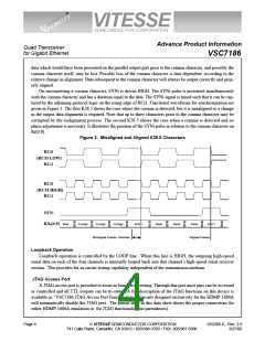
VITESSE
SEMICONDUCTOR CORPORATION
Advance Product Information
Quad Transceiver
for Gigabit Ethernet
VSC7186
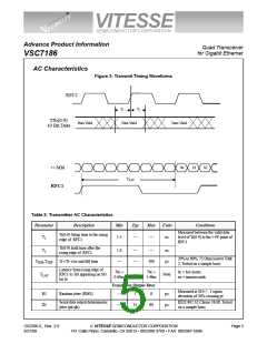
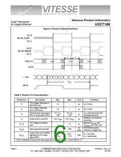
Figure 4: Receive Timing Waveforms
RCi0
RCM=LOW
RCi1
RCi0
RCM=HIGH
RCi1
T
T
2
1
VALID
VALID
VALID
RXi(0:9)
SYNi
S0
S1
S2
+/-SIi
RCi1
RLAT
Table 3: Receive AC Characteristics—
Parameters
Description
Min.
Max.
Units
Conditions
TTL Outputs Valid prior to
RCi1/RCi0 rise
T1
3.0
2.0
—
ns.
@ 1.25Gb/s
@ 1.25Gb/s
TTL Outputs Valid after
RCi1 or RCi0 rise
T2
T3
—
ns.
ps.
ps.
ns.
Delay between rising edge of
RCi1 to rising edge of RCi0
10 x TRi
-500
10 x TRi
+500
TRi is the bit period of the
incoming data on Ri.
Whether or not locked to
serial data.
T4
Period of RCi1 and RCi0
1.98 x TREF
2.02 x TREF
2.4
TTL Output rise and fall
time
Between VIL(max) and
TR, TF
TLOCK
—
—
VIH(min), into 10 pf. load.
bit
times
8b/10b IDLE pattern.
Tested on a sample basis
Data acquisition lock time*
1400
Latency from bit 0 of RXi0
appearing on SI to rising
edge of RCi1
12bc +
2.77ns
13bc +
7.28
bc = bit clocks
ns = nanoseconds.
RLAT
Note:
* Note: Probability of recovery for data acquisition is 95% per Section 5.3 of FC-PH rev. 4.3
Page 6
VITESSE SEMICONDUCTOR CORPORATION
741 Calle Plano, Camarillo, CA 93012 • 805/388-3700 • FAX: 805/987-5896
G52306-0, Rev. 2.0
3/27/00

 VITESSE [ VITESSE SEMICONDUCTOR CORPORATION ]