VITESSE
SEMICONDUCTOR CORPORATION
Advance Product Information
Quad Transceiver
for Gigabit Ethernet
VSC7186
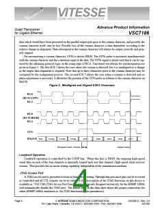
AC Characteristics
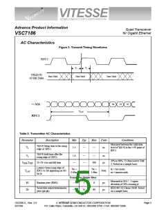
Figure 3: Transmit Timing Waveforms
RFC1
T
T
2
1
TXi(0:9)
10 Bit Data
Data Valid
Data Valid
Data Valid
S0
S1
S2
+/-SOi
RFC1
T
LAT
Table 2: Transmitter AC Characteristics
Parameter
Description
Min
Typ
Max
Units
Conditions
Measured between the valid data
level of Ti(0:9) to the 1.4V point of
RFC1
Ti(0:9) Setup time to the rising
edge of RFC1
T1
1.5
—
—
ns.
Ti(0:9) hold time after the
rising edge of RFC1
T2
1.0
—
—
—
ns.
ps.
20% to 80%, 75 Ohm load to Vdd/
2, Tested on a sample basis
T
SDR,TSDF
Ti+/Ti- rise and fall time
—
300
Latency from rising edge of
RFC1 to Ti0 appearing on SO
bit 0i
7bc +
0.66ns
7bc +
1.46ns
bc = bit clocks
ns = nanoseconds
TLAT
—
Note:
Transmitter Output Jitter
Measured at SO+/-, 1 sigma
deviation of 50% crossing pt
RJ
DJ
Random jitter (RMS)
—
—
5
8
ps.
ps.
Serial data output deterministic
jitter (pk-pk)
IEEE 802.3Z Clause 38.68, Tested
on a sample basis
35
80
G52306-0, Rev. 2.0
3/27/00
VITESSE SEMICONDUCTOR CORPORATION
741 Calle Plano, Camarillo, CA 93012 • 805/388-3700 • FAX: 805/987-5896
Page 5

 VITESSE [ VITESSE SEMICONDUCTOR CORPORATION ]