VITESSE
SEMICONDUCTOR CORPORATION
Advance Product Information
Quad Transceiver
for Gigabit Ethernet
VSC7186
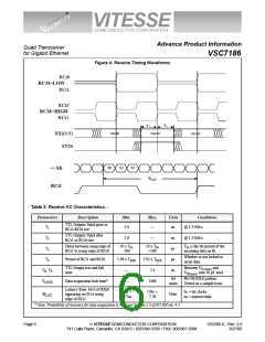
data which would have been presented on the parallel output port prior to the comma character, and possibly the
comma character itself, may be lost. Possible loss of the comma character is data dependent, according to the
relative change in alignment. Data subsequent to the comma character will always be output correctly and prop-
erly aligned.
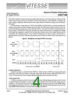
On encountering a comma character, SYNi is driven HIGH. The SYNi pulse is presented simultaneously
with the comma character and has a duration equal to the data. The SYNi signal is timed such that it can be cap-
tured by the adjoining protocol logic on the rising edge of RCi1. Functional waveforms for synchronization are
given in Figure 1. The first K28.5 shows the case where the comma is detected, but it is misaligned so a change
in the output data alignment is required. Note that up to three characters prior to the comma character may be
corrupted by the realignment process. The second K28.5 shows the case when a comma is detected and no
phase adjustment is necessary. It illustrates the position of the SYNi pulse in relation to the comma character on
Ri(0:9).
Figure 2: Misaligned and Aligned K28.5 Characters
RCi0
(RCM LOW)
RCi1
RCi0
(RCM HIGH)
RCi1
SYNi
Data
Corrupt
Corrupt
Corrupt
K28.5
Data1
Data2
Data3
K28.5
RXi(0:9)
Aligned Comma
Misaligned Comma: Stretched
Loopback Operation
Loopback operation is controlled by the LOOP line. When this line is HIGH, the outgoing high-speed
serial data on each of the four channels is internally looped back into that channel’s high-speed serial receiver
section. This provides for in-circuit testing capability independent of the transmission medium.
JTAG Access Port
A JTAG access port is provided to assist in board-level testing. Through this port most pins can be accessed
or controlled and all TTL outputs can be tri-stated. A full description of the JTAG functions on this device is
available in “VSC7186 JTAG Access Port Functionality”. Circuits designed exclusively for the HDMP-1686A
will automatically disable the JTAG port. The pinout table in this data sheet shows the proper connections for
either HDMP-1686A emulation or for JTAG functionality (in parentheses).
Page 4
VITESSE SEMICONDUCTOR CORPORATION
741 Calle Plano, Camarillo, CA 93012 • 805/388-3700 • FAX: 805/987-5896
G52306-0, Rev. 2.0
3/27/00

 VITESSE [ VITESSE SEMICONDUCTOR CORPORATION ]