VSC6134
Datasheet
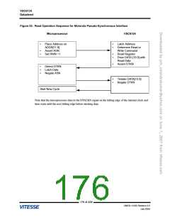
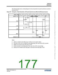
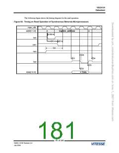
The following figure shows a timing diagram for the read operation for pseudo-synchronous motorola
microprocessors.
Figure 56. Timing for a Read Operation of Pseudo-Synchronous Motorola Microprocessors
mpu_clk
addr[11:0]
asn
register_address
S1
S0
S4
S2
D0
S3
csn
rwn
D6
D5
D2
D1
D4
dtkn
D3
data[15:0]
Data
Notes:
●
●
●
●
●
Address is latched on the falling edge of ASN into level-sensitive latches.
The start of a bus cycle is recognized on the falling edge of the clock when ASN is asserted.
DTKN is de-asserted on the rising edge of ASN.
DTKN is tristated on the falling edge of the clock when ASN is detected high.
DATA[15:0] is tristated on the rising edge of ASN and on the rising edge of CSN.
177 of 438
VMDS-10185 Revision 4.0
July 2006

 VITESSE [ VITESSE SEMICONDUCTOR CORPORATION ]