6N137 / VO2601 / 11 / VO2630 / 31 / VO4661
Vishay Semiconductors
Switching Characteristics
Over Recommended Temperature (Ta = - 40 to + 100 °C), VCC = 5 V, IF = 7.5 mA unless otherwise specified.
All Typicals at Ta = 25 °C, VCC = 5 V.
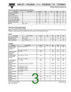
Parameter
Test condition
Symbol
tPLH
Min
20
Typ.
48
Max
75*
Unit
ns
Propagation delay time to high RL = 350 Ω, CL = 15 pF
output level
tPLH
tPHL
100
75*
ns
ns
Propagation delay time to low
output level
RL = 350 Ω, CL = 15 pF
25
50
tPHL
100
35
ns
ns
ns
ns
ns
ns
Pulse width distortion
RL = 350 Ω, CL = 15 pF
RL = 350 Ω, CL = 15 pF
RL = 350 Ω, CL = 15 pF
RL = 350 Ω, CL = 15 pF
| tPHL - tPLH
|
2.9
8
Propagation delay skew
Output rise time (10 - 90 %)
Output fall time (90 - 10 %)
tPSK
tr
40
23
7
tf
Propagation delay time of
enable from VEH to VEL
RL = 350 Ω, CL = 15 pF,
VEL = 0 V, VEH = 3 V
tELH
12
Propagation delay time of
enable from VEL to VEH
RL = 350 Ω, CL = 15 pF,
VEL = 0 V, VEH = 3 V
tEHL
11
ns
* 75 ns applies to the 6N137 only, a JEDEC registered specification
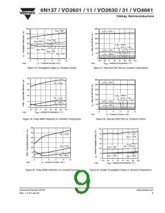
V
CC
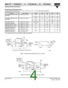
Single Channel
Pulse Gen.
= 50 Ω
f
V
1
2
3
4
CC 8
R
L
Z
t
o
= 7.5 mA
F
I
F
I
I
V
E
= t = 5 ns
r
= 3.75 mA
Input I
7
6
5
F
F
0.1 µF
Bypass
0 mA
Output V
Monitoring
Node
V
OUT
O
Input I
Monitoring
F
V
OH
Output V
O
1.5 V
OL
Node
R
V
C
= 15 pF
M
L
GND
t
PHL
t
PLH
The Probe and Jig Capacitances are included in C
L
18964-2
Figure 1. Single Channel Test Circuit for tPLH, tPHL, tr and tf
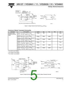
Pulse Gen.
Z
t
= 50 Ω
r
o
f
V
CC
= t = 5 ns
Dual Channel
I
F
V
1
2
3
4
8
7
6
5
CC
R
L
Output V
O
Input
Monitoring
Monitoring
Node
R
Node
0.1 µF
Bypass
= 15 pF
C
M
L
GND
18963-2
Figure 2. Dual Channel Test Circuit for tPLH, tPHL, tr and tf
www.vishay.com
4
Document Number 84732
Rev. 1.0, 07-Jun-05

 VISHAY [ VISHAY ]